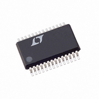
LTC1410CG Linear Technology, LTC1410CG Datasheet

LTC1410CG
Specifications of LTC1410CG
Available stocks
Related parts for LTC1410CG
LTC1410CG Summary of contents
Page 1
... The ADC has a P compatible, 12-bit parallel output port. There is no pipeline delay in the conversion results. A separate convert start input and a data ready signal (BUSY) ease connections to FIFOs, DSPs and microprocessors. , LTC and LT are registered trademarks of Linear Technology Corporation – ...
Page 2
... C. With Internal Reference (Notes CONDITIONS (Note 7) (Note OUT(REF) CONDITIONS 4.75V V 5.25V, – 5.25V High Between Conversions During Conversions – 2.5V < (– < 2. ORDER TOP VIEW PART NUMBER LTC1410CG LTC1410CSW 4 25 BUSY LTC1410IG 6 23 CONVST LTC1410ISW SHDN 9 20 NAP/SLP 10 19 OGND ...
Page 3
ACCURACY otherwise specifications are (Note 5) A SYMBOL PARAMETER S/( Signal-to-(Noise + Distortion) Ratio THD Total Harmonic Distortion Peak Harmonic or Spurious Noise IMD Intermodulation Distortion Full Power ...
Page 4
LTC1410 W U POWER REQUIRE E TS otherwise specifications are (Note 5) A SYMBOL PARAMETER P Power Dissipation D Nap Mode Sleep Mode CHARACTERISTICS range, otherwise specifications are at T ...
Page 5
W U TYPICAL PERFORMANCE CHARACTERISTICS S/( Input Frequency and Amplitude 0dB –20dB –60dB 1.25MHz SAMPLE 0 1k 10k ...
Page 6
LTC1410 CTIO (Pin 1): Positive Analog Input, 2.5V. IN – A (Pin 2): Negative Analog Input, 2.5V (Pin 3): 2.50V Reference Output. REF REFCOMP (Pin 4): 4.06V Reference Bypass Pin. ...
Page 7
TEST CIRCUITS Load Circuits for Access Timing DBN DBN (A) Hi AND (B) Hi APPLICATIONS INFORMATION CONVERSION DETAILS The LTC1410 uses a successive approximation algorithm ...
Page 8
LTC1410 U U APPLICATIONS INFORMATION DYNAMIC PERFORMANCE The LTC1410 has excellent high speed sampling capabil- ity. Fast Four Transform (FFT) test techniques are used to test the ADC’s frequency response, distortion and noise at the rated throughput. By applying a ...
Page 9
U U APPLICATIONS INFORMATION where V is the RMS amplitude of the fundamental fre- 1 quency and V through V are the amplitudes of the 2 n second through nth harmonics. THD vs Input Frequency is shown in Figure 4. ...
Page 10
LTC1410 U U APPLICATIONS INFORMATION capacitors at the end of conversion. During conversion the analog inputs draw only a small leakage current. If the source impedance of the driving circuit is low then the LTC1410 inputs can be driven directly. ...
Page 11
U U APPLICATIONS INFORMATION easily overdriven in applications where an external refer- ence is required. The reference amplifier provides buffer- ing between the internal reference and the capacitive DAC. The reference amplifier compensation pin REFCOMP (Pin 4), must be bypassed ...
Page 12
LTC1410 U U APPLICATIONS INFORMATION High quality tantalum and ceramic bypass capacitors should be used at the and REFCOMP pins shown in the Typical Application on the first page of this data sheet. Bypass ...
Page 13
U U APPLICATIONS INFORMATION Power Shutdown The LTC1410 provides two power shutdown modes, Nap and Sleep, to save power during inactive periods. The Nap mode reduces the power by 95% and leaves only the digital logic and reference powered up. ...
Page 14
LTC1410 U U APPLICATIONS INFORMATION CONVST BUSY DATA Figure 14. Mode 1a. CONVST Starts a Conversion. Data Outputs Always Enabled (CONVST = CONVST BUSY DATA (N – 1) ...
Page 15
... FLASH SHALL NOT EXCEED 0.010" (0.254mm) PER SIDE Information furnished by Linear Technology Corporation is believed to be accurate and reliable. However, no responsibility is assumed for its use. Linear Technology Corporation makes no represen- tation that the interconnection of its circuits as described herein will not infringe on existing patent rights. ...
Page 16
... S28 (WIDE) 0996 300ksps SAMPLE 100ksps 140ksps SAMPLE 1410fa LT/TP 0399 2K REV A • PRINTED IN USA LINEAR TECHNOLOGY CORPORATION 1995 ...


