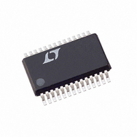
LTC1415CG#TRPBF Linear Technology, LTC1415CG#TRPBF Datasheet - Page 6

LTC1415CG#TRPBF
Manufacturer Part Number
LTC1415CG#TRPBF
Description
IC A/D CONV 12BIT SAMPLNG 28SSOP
Manufacturer
Linear Technology
Datasheet
1.LTC1415CSWPBF.pdf
(24 pages)
Specifications of LTC1415CG#TRPBF
Number Of Bits
12
Sampling Rate (per Second)
1.25M
Data Interface
Parallel
Number Of Converters
1
Power Dissipation (max)
100mW
Voltage Supply Source
Single Supply
Operating Temperature
0°C ~ 70°C
Mounting Type
Surface Mount
Package / Case
28-SSOP (0.200", 5.30mm Width)
Lead Free Status / RoHS Status
Lead free / RoHS Compliant
Available stocks
Company
Part Number
Manufacturer
Quantity
Price
PI FU CTIO S
LTC1415
TYPICAL PERFORMANCE CHARACTERISTICS
+ A
– A
V
REFCOMP (Pin 4): Bypass to AGND with 10 F tantalum
in parallel with 0.1 F or 10 F ceramic.
AGND (Pin 5): Analog Ground.
D11 to D4 (Pins 6 to 13): Three-State Data Outputs.
DGND (Pin 14): Digital Ground.
D3 to D0 (Pins 15 to 18): Three-State Data Outputs.
OGND (Pin 19): Digital Output Buffer Ground.
NAP/SLP (Pin 20): Power Shutdown Mode. High for
quick wake-up Nap mode.
SHDN (Pin 21): Power Shutdown Input. A low logic
level will invoke the Shutdown mode selected by the
NAP/SLP pin. Tie high if unused.
6
REF
U
IN
IN
(Pin 3): 2.50V Reference Output.
(Pin 1): Positive Analog Input, 0V to 4.096V.
(Pin 2): Negative Analog Input, 0V to 4.096V.
–100
U
–10
–20
–30
–40
–50
–60
–70
–80
–90
0
1k
Power Supply Feedthrough vs
Ripple Frequency
U
RIPPLE FREQUENCY (Hz)
10k
V
DD
W
DGND
100k
U
OV
DD
LTC1415 • TPC08
1M
2M
RD (Pin 22): Read Input. This enables the output
drivers when CS is low.
CONVST (Pin 23): Conversion Start Signal. This active
low signal starts a conversion on its falling edge.
CS (Pin 24): The Chip Select input must be low for the
ADC to recognize CONVST and RD inputs.
BUSY (Pin 25): The BUSY output shows the converter
status. It is low when a conversion is in progress. Its
rising edge may be used to latch the output data.
0V
28 for 5V output. Tie to 3V for driving 3V logic.
DV
AV
with 10 F tantalum in parallel with 0.1 F or 10 F
ceramic.
DD
DD
DD
(Pin 26): Digital output buffer supply. Short to Pin
(Pin 27): 5V Positive Supply. Short to Pin 28.
(Pin 28): 5V Positive Supply. Bypass to AGND
80
70
60
50
40
30
20
10
0
1k
Input Common Mode Rejection
vs Input Frequency
INPUT FREQUENCY (Hz)
10k
100k
LTC1415 • TPC09
1M 2M


