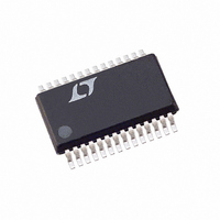
LTC1412IG Linear Technology, LTC1412IG Datasheet - Page 6

LTC1412IG
Manufacturer Part Number
LTC1412IG
Description
IC A/D CONV 12BIT SAMPLNG 28SSOP
Manufacturer
Linear Technology
Datasheet
1.LTC1412CGPBF.pdf
(16 pages)
Specifications of LTC1412IG
Number Of Bits
12
Sampling Rate (per Second)
3M
Data Interface
Parallel
Number Of Converters
1
Power Dissipation (max)
220mW
Voltage Supply Source
Dual ±
Operating Temperature
-40°C ~ 85°C
Mounting Type
Surface Mount
Package / Case
28-SSOP (0.200", 5.30mm Width)
Lead Free Status / RoHS Status
Contains lead / RoHS non-compliant
Available stocks
Company
Part Number
Manufacturer
Quantity
Price
Part Number:
LTC1412IG#PBF
Manufacturer:
LINEAR/凌特
Quantity:
20 000
TYPICAL PERFOR A CE CHARACTERISTICS
LTC1412
PIN
A
when A
driven.
A
driven differentially with A
V
REFCOMP (Pin 4): 4.06V Reference Bypass Pin.
Bypass to AGND with 10 F ceramic (or 10 F tantalum in
parallel with 0.1 F ceramic).
AGND (Pin 5): Analog Ground.
D11 to D4 (Pins 6 to 13): Three-State Data Outputs.
DGND (Pin 14): Digital Ground for Internal Logic.
D3 to D0 (Pins 15 to 18): Three-State Data Outputs.
DGND (Pin 19): Digital Ground for Internal Logic.
DV
to AGND with 0.1 F ceramic.
6
IN
IN
REF
DD
U
+
–
(Pin 2): Negative Analog Input. Can be grounded or
(Pin 1): Positive Analog Input. 2.5V input range
(Pin 3): 2.5V Reference Output.
(Pin 20): 5V Positive Supply. Tie to Pin 28. Bypass
FUNCTIONS
IN
–100
–120
– 20
– 40
– 60
– 80
–
U
0
is grounded.
1k
Power Supply Feedthrough
vs Ripple Frequency
10k
RIPPLE FREQUENCY (Hz)
U
IN
100k
V
W
SS
+
2.5V differential if A
.
U
1M
V
DGND
DD
1412 G08
10M
IN
–
is
OV
to Pin 28 when driving 5V logic. Tie to 3V when driving
3V logic.
OGND (Pin 22): Digital Ground for the Output Drivers.
CONVST (Pin 23): Conversion Start Signal. This active low
signal starts a conversion on its falling edge.
CS (Pin 24): Chip Select. This input must be low for the
ADC to recognize the CONVST inputs.
BUSY (Pin 25): The BUSY Output Shows the Converter
Status. It is low when a conversion is in progress.
V
10 F ceramic (or 10 F tantalum in parallel with 0.1 F
ceramic).
DV
AV
10 F ceramic (or 10 F tantalum in parallel with 0.1 F
ceramic).
SS
DD
DD
DD
(Pin 26): – 5V Negative Supply. Bypass to AGND with
(Pin 21): Positive Supply for the Output Drivers. Tie
(Pin 28): 5V Positive Supply. Bypass to AGND with
(Pin 27): 5V Positive Supply. Tie to Pin 28.
80
70
60
50
40
30
20
10
0
1k
Input Common Mode Rejection
vs Input Frequency
10k
INPUT FREQUENCY (Hz)
100k
1M
1412 G09
10M


