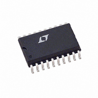
LTC1609ISW Linear Technology, LTC1609ISW Datasheet - Page 8

LTC1609ISW
Manufacturer Part Number
LTC1609ISW
Description
IC A/DCONV 16BIT SRL SAMP 20SOIC
Manufacturer
Linear Technology
Datasheet
1.LTC1609CSW.pdf
(24 pages)
Specifications of LTC1609ISW
Number Of Bits
16
Sampling Rate (per Second)
200k
Data Interface
Serial
Number Of Converters
1
Power Dissipation (max)
100mW
Voltage Supply Source
Analog and Digital
Operating Temperature
-40°C ~ 85°C
Mounting Type
Surface Mount
Package / Case
20-SOIC (0.300", 7.50mm Width)
Lead Free Status / RoHS Status
Contains lead / RoHS non-compliant
Available stocks
Company
Part Number
Manufacturer
Quantity
Price
Company:
Part Number:
LTC1609ISW
Manufacturer:
SONY
Quantity:
6 232
Part Number:
LTC1609ISW
Manufacturer:
LT/凌特
Quantity:
20 000
Company:
Part Number:
LTC1609ISW#PBF
Manufacturer:
Linear Technology
Quantity:
135
FUNCTIONAL BLOCK DIAGRA
APPLICATIO S I FOR ATIO
LTC1609
Conversion Details
The LTC1609 uses a successive approximation algorithm
and an internal sample-and-hold circuit to convert an
analog signal to a 16-bit serial output. The ADC is complete
with a precision reference and an internal clock. The
control logic provides easy interface to microprocessors
and DSPs. (Please refer to the Digital Interface section for
timing information.)
Conversion start is controlled by the CS and R/C inputs. At
the start of conversion the successive approximation
register (SAR) is reset. Once a conversion cycle has begun
it cannot be restarted.
During the conversion, the internal 16-bit capacitive DAC
output is sequenced by the SAR from the most significant
bit (MSB) to the least significant bit (LSB). Referring to
Figure 1, V
the sample-and-hold capacitor during the acquire phase
and the comparator offset is nulled by the autozero switches.
In this acquire phase, a minimum delay of 2 s will provide
enough time for the sample-and-hold capacitor to acquire
8
U
AGND1
AGND2
(2.5V)
DGND
R1
R2
R3
CAP
REF
IN
IN
IN
IN
is connected through the resistor divider to
U
20k
10k
5k
4k
U
REF BUF
2.5V REF
U
INTERNAL
CLOCK
20k
W
U
16-BIT CAPACITIVE DAC
SUCCESSIVE APPROXIMATION
CS
W
C
C
SAMPLE
SAMPLE
CONTROL LOGIC
REGISTER
R/C
V
the analog signal. During the convert phase, the autozero
switches open, putting the comparator into the compare
mode. The input switch switches C
injecting the analog input charge onto the summing junc-
tion. This input charge is successively compared with the
binary-weighted charges supplied by the capacitive DAC.
Bit decisions are made by the high speed comparator. At
IN
PWRD
R
IN1
R
IN2
Figure 1. LTC1609 Simplified Equivalent Circuit
BUSY
SAMPLE
HOLD
ZEROING SWITCHES
+
–
COMP
SB/BTC
C
SAMPLE
C
V
DAC
DAC
SERIAL INTERFACE
EXT/INT
DAC
TAG
SAMPLE
–
+
SAMPLE
1609 BD
COMPARATOR
SI
SHIFT REGISTER
DATA
DATACLK
SYNC
V
V
to ground,
ANA
DIG
16-BIT
S
A
R
1609fa
1609 F01


