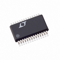
LTC1605-1CG Linear Technology, LTC1605-1CG Datasheet - Page 16

LTC1605-1CG
Manufacturer Part Number
LTC1605-1CG
Description
IC A/D CONV 16BIT SAMPLNG 28SSOP
Manufacturer
Linear Technology
Datasheet
1.LTC1605-1CGPBF.pdf
(20 pages)
Specifications of LTC1605-1CG
Number Of Bits
16
Sampling Rate (per Second)
100k
Data Interface
Parallel
Number Of Converters
1
Power Dissipation (max)
80mW
Voltage Supply Source
Analog and Digital
Operating Temperature
0°C ~ 70°C
Mounting Type
Surface Mount
Package / Case
28-SSOP (0.200", 5.30mm Width)
Lead Free Status / RoHS Status
Contains lead / RoHS non-compliant
Available stocks
Company
Part Number
Manufacturer
Quantity
Price
Part Number:
LTC1605-1CG#PBF
Manufacturer:
LINEAR/凌特
Quantity:
20 000
Part Number:
LTC1605-1CG#TRPBF
Manufacturer:
LINEAR/凌特
Quantity:
20 000
LTC1605-1/LTC1605-2
*****************************************
* Start GETDATA Routine
*****************************************
*
INIT1
*
*
*
*
*
* DDRD’s Bit5 is a 1 so that port D’s SS* pin is a general output
*
*
*
*
GETDATAPSHX
*
*****************************************
* Setup indecies
*****************************************
*
*
*
*****************************************
* Ensure that a logic high is applied
* to the LTC1391’s /CS and the
* LTC1605’s R/C pins
*****************************************
*
*
*
*
*
*
*
*****************************************
TYPICAL APPLICATIO S
16
ORG
LDAA
STAA
LDAA
STAA
LDAA
STAA
LDAA
STAA
LDAA
STAA
PSHY
PSHA
LDX
LDY
BSET
BSET
$C000
#$03
PIOC
#$00
DDRC
#$2F
PORTD
#$38
DDRD
#$50
SPCR
#$0
#$1000
PORTD,Y %00100000
PORTA,Y %00010000
Program start location
0,0,0,0,0,0,1,1
“STAF=0,STAI=0,CWOM=0,HNDS=0, OIN=0, PLS=0, EGA=1,INVB=1”
Ensures that the PIOC register’s status is the same
as after a reset, necessary of simple Port D manipulation
0,0,0,0,0,0,0,0
“Bits 7 - 0 are used as inputs for the LTC1605’s data
Direction of PortD’s bit are now set as inputs
-,-,1,0;1,1,1,1
-, -, SS*-Hi, SCK-Lo, MOSI-Hi, MISO-Hi, X, X
Keeps SS* a logic high when DDRD, Bit5 is set
-,-,1,1;1,0,0,0
SS* , SCK, MOSI are configured as Outputs
MISO, TxD, RxD
The SPI is configured as Master, CPHA = 0, CPOL = 0
and the clock rate is E/2
(This assumes an E-Clock frequency of 4MHz. For higher
E-Clock frequencies, change the above value of $50 to a
value that ensures the SCK frequency is 2MHz or less.)
The X register is used as a pointer to the memory
locations that hold the conversion data
U
*
*
This sets the SS* output bit to a logic
high, ensuring that the LTC1391’s CS*
input is a logic high while clocking
MUX address data into the LTC1391
This sets the R/C* output bit to a logic
high, ensuring that the LTC1605’s R/C*
input is a logic high before initiating
a conversion
are configured as Inputs
*
*
*


