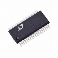
LTC1604AIG Linear Technology, LTC1604AIG Datasheet - Page 14

LTC1604AIG
Manufacturer Part Number
LTC1604AIG
Description
IC CONV A/D 16BIT SAMPLNG 36SSOP
Manufacturer
Linear Technology
Datasheet
1.LTC1604CGPBF.pdf
(20 pages)
Specifications of LTC1604AIG
Number Of Bits
16
Sampling Rate (per Second)
333k
Data Interface
Parallel
Number Of Converters
1
Power Dissipation (max)
350mW
Voltage Supply Source
Dual ±
Operating Temperature
-40°C ~ 85°C
Mounting Type
Surface Mount
Package / Case
36-SSOP (0.200", 5.30mm Width)
Lead Free Status / RoHS Status
Contains lead / RoHS non-compliant
Available stocks
Company
Part Number
Manufacturer
Quantity
Price
Part Number:
LTC1604AIG#TRPBF
Manufacturer:
LINEAR/凌特
Quantity:
20 000
APPLICATIONS
LTC1604
can not exceed the AV
Integral nonlinearity errors (INL) and differential nonlin-
earity errors (DNL) are independent of the common mode
voltage, however, the bipolar zero error (BZE) will vary.
The change in BZE is typically less than 0.1% of the
common mode voltage. Dynamic performance is also
affected by the common mode voltage. THD will degrade
as the inputs approach either power supply rail, from 96dB
with a common mode of 0V to 86dB with a common mode
of 2.5V or – 2.5V.
Differential inputs allow greater flexibility for accepting
different input ranges. Figure 14b shows a circuit that
converts a 0V to 5V analog input signal with only an
additional buffer that is not in the signal path.
14
LTC1450
Figure 14a. CMRR vs Input Frequency
80
70
60
50
40
30
20
10
0
Figure 13. Driving V
1k
U
INPUT FREQUENCY (Hz)
DD
ANALOG INPUT
10k
DIFFERENTIAL
INFORMATION
2V TO 2.7V
2V TO 2.7V
or V
U
47 F
SS
REF
100k
power supply voltages.
with a DAC
W
1
2
3
4
5
A
A
V
REFCOMP
AGND
IN
IN
REF
+
–
1604 G14a
LTC1604
1M
U
1604 F13
Full-Scale and Offset Adjustment
Figure 15a shows the ideal input/output characteristics
for the LTC1604. The code transitions occur midway
between successive integer LSB values (i.e., – FS +
0.5LSB, – FS + 1.5LSB, – FS + 2.5LSB,... FS – 1.5LSB,
FS – 0.5LSB). The output is two’s complement binary with
1LSB = FS – (– FS)/65536 = 5V/65536 = 76.3 V.
In applications where absolute accuracy is important,
offset and full-scale errors can be adjusted to zero. Offset
error must be adjusted before full-scale error. Figure 15b
shows the extra components required for full-scale error
adjustment. Zero offset is achieved by adjusting the offset
applied to the A
Figure 14b. Selectable 0V to 5V or 2.5V Input Range
2.5V
Figure 15a. LTC1604 Transfer Characteristics
011...111
011...110
000...001
000...000
111...111
111...110
100...001
100...000
– (FS – 1LSB)
0V TO
5V
IN
ANALOG INPUT
–
INPUT VOLTAGE (A
input. For zero offset error apply
10 F
+
–
4
5
1
2
3
A
A
V
REFCOMP
AGND
IN
IN
REF
IN
+
–
+
LTC1604
– A
IN
–
FS – 1LSB
)
1604 F14b
1604 F15a


