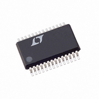
LTC1605ACG#PBF Linear Technology, LTC1605ACG#PBF Datasheet - Page 4

LTC1605ACG#PBF
Manufacturer Part Number
LTC1605ACG#PBF
Description
IC A/D CONV 16BIT SAMPLNG 28SSOP
Manufacturer
Linear Technology
Datasheet
1.LTC1605INPBF.pdf
(16 pages)
Specifications of LTC1605ACG#PBF
Number Of Bits
16
Sampling Rate (per Second)
100k
Data Interface
Parallel
Number Of Converters
1
Power Dissipation (max)
80mW
Voltage Supply Source
Analog and Digital
Operating Temperature
0°C ~ 70°C
Mounting Type
Surface Mount
Package / Case
28-SSOP (0.200", 5.30mm Width)
Lead Free Status / RoHS Status
Lead free / RoHS Compliant
Available stocks
Company
Part Number
Manufacturer
Quantity
Price
DIGITAL INPUTS AND DIGITAL OUTPUTS
operating temperature range, otherwise specifications are at T
range, otherwise specifications are at T
otherwise specifications are at T
LTC1605
SYMBOL
V
I
C
I
I
TIMING CHARACTERISTICS
SYMBOL
f
t
t
t
t
t
t
t
t
t
t
t
t
t
t
POWER REQUIREMENTS
SYMBOL
V
I
P
Note 1: Stresses beyond those listed under Absolute Maximum Ratings
may cause permanent damage to the device. Exposure to any Absolute
Maximum Rating condition for extended periods may affect device
reliability and lifetime.
Note 2: All voltage values are with respect to ground with DGND, AGND1
and AGND2 wired together (unless otherwise noted).
Note 3: When these pin voltages are taken below ground or above V
V
handle input currents of greater than 100mA below ground or above V
without latch-up.
4
OZ
SOURCE
SINK
SAMPLE(MAX)
CONV
ACQ
1
2
3
4
5
6
7
8
9
10
11
12
DD
OL
OZ
DD
DIS
DIG
W U
= V
DD
, they will be clamped by internal diodes. This product can
PARAMETER
Low Level Output Voltage
Hi-Z Output Leakage D15 to D0
Hi-Z Output Capacitance D15 to D0
Output Source Current
Output Sink Current
PARAMETER
Maximum Sampling Frequency
Conversion Time
Acquisition Time
Convert Pulse Width
Data Valid Delay After R/C↓
BUSY Delay from R/C↓
BUSY Low
BUSY Delay After End of Conversion
Aperture Delay
Bus Relinquish Time
BUSY Delay After Data Valid
Previous Data Valid After R/C↓
R/C to CS Setup Time
Time Between Conversions
Bus Access and Byte Delay
PARAMETER
Positive Supply Voltage
Positive Supply Current
Power Dissipation
U
A
W U
= 25°C. (Note 5)
U
A
= 25°C. (Note 5)
CONDITIONS
V
V
CS High (Note 9)
V
V
The
DD
OUT
OUT
OUT
CONDITIONS
(Note 11)
(Note 9)
C
(Notes 9, 10)
(Notes 9, 10)
CONDITIONS
(Notes 9, 10)
L
= 4.75V
= 50pF
= 0V to V
= 0V
= V
The
●
denotes specifications which apply over the full operating temperature range,
DD
●
ANA
denotes specifications which apply over the full operating temperature
DD
DD
A
=
, CS High
= 25°C. (Note 5)
Note 4: When these pin voltages are taken below ground, they will be
clamped by internal diodes. This product can handle input currents of
90mA below ground without latchup. These pins are not clamped to V
Note 5: V
specified.
Note 6: Linearity, offset and full-scale specifications apply for a V
with respect to ground.
Note 7: Integral nonlinearity is defined as the deviation of a code from a
straight line passing through the actual end points of the transfer curve.
The deviation is measured from the center of the quantization band.
DD
I
I
The
O
O
= 5V, f
= 160µA
= 1.6mA
●
denotes specifications which apply over the full
SAMPLE
= 100kHz, t
●
●
●
●
●
●
●
●
●
●
●
●
4.75
MIN
MIN
MIN
100
40
10
50
10
10
10
LTC1605/LTC1605A
LTC1605/LTC1605A
LTC1605/LTC1605A
r
= t
f
= 5ns unless otherwise
0.05
0.10
TYP
–10
TYP
220
200
TYP
7.4
10
40
35
11
55
MAX
MAX
MAX
5.25
±10
0.4
15
65
83
83
16
80
8
2
8
8
IN
input
UNITS
UNITS
UNITS
1605fc
DD
mW
kHz
mA
mA
mA
µA
pF
µs
µs
ns
µs
ns
µs
ns
ns
ns
ns
µs
ns
µs
ns
.
V
V
V


