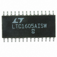
LTC1605AISW#PBF Linear Technology, LTC1605AISW#PBF Datasheet - Page 6

LTC1605AISW#PBF
Manufacturer Part Number
LTC1605AISW#PBF
Description
IC A/D CONV 16BIT SAMPLNG 28SOIC
Manufacturer
Linear Technology
Datasheet
1.LTC1605INPBF.pdf
(16 pages)
Specifications of LTC1605AISW#PBF
Number Of Bits
16
Sampling Rate (per Second)
100k
Data Interface
Parallel
Number Of Converters
1
Power Dissipation (max)
80mW
Voltage Supply Source
Analog and Digital
Operating Temperature
-40°C ~ 85°C
Mounting Type
Surface Mount
Package / Case
28-SOIC (0.300", 7.50mm Width)
Number Of Elements
1
Resolution
16Bit
Architecture
SAR
Sample Rate
100KSPS
Input Polarity
Bipolar
Input Type
Voltage
Rated Input Volt
±10V
Differential Input
No
Power Supply Requirement
Analog and Digital
Single Supply Voltage (typ)
5V
Single Supply Voltage (min)
4.75V
Single Supply Voltage (max)
5.25V
Dual Supply Voltage (typ)
Not RequiredV
Dual Supply Voltage (min)
Not RequiredV
Dual Supply Voltage (max)
Not RequiredV
Power Dissipation
80mW
Differential Linearity Error
1LSB
Integral Nonlinearity Error
±2LSB
Operating Temp Range
-40C to 85C
Operating Temperature Classification
Industrial
Mounting
Surface Mount
Pin Count
28
Package Type
SOIC W
Input Signal Type
Single-Ended
Lead Free Status / RoHS Status
Lead free / RoHS Compliant
Available stocks
Company
Part Number
Manufacturer
Quantity
Price
LTC1605
TYPICAL PERFORMANCE CHARACTERISTICS
PIN
V
resistor to the analog input. Full-scale input range is
±10V.
AGND1 (Pin 2): Analog Ground. Tie to analog ground
plane.
REF (Pin 3): 2.5V Reference Output. Bypass with 2.2µF
tantalum capacitor. Can be driven with an external refer-
ence.
CAP (Pin 4): Reference Buffer Output. Bypass with 2.2µF
tantalum capacitor.
6
IN
U
(Pin 1): Analog Input. Connect through a 200Ω
FUNCTIONS
U
90
89
88
87
86
85
84
83
82
81
1
SINAD vs Input Frequency
U
INPUT FREQUENCY (kHz)
–100
–110
–120
–130
–10
–20
–30
–40
–50
–60
–70
–80
–90
0
W
0
LTC1605 Nonaveraged 4096 Point FFT Plot
10
U
f
5
SAMPLE
SINAD = 87.5dB
THD = –101.7dB
f
IN
1605 • TPC08
= 100kHz
= 1kHz
10
100
15
20
FREQUENCY (kHz)
AGND2 (Pin 5): Analog Ground. Tie to analog ground
plane.
D15 to D8 (Pins 6 to 13): Three-State Data Outputs.
Hi-Z state when CS is high or when R/C is low.
DGND (Pin 14): Digital Ground.
D7 to D0 (Pins 15 to 22): Three-State Data Outputs.
Hi-Z state when CS is high or when R/C is low.
BYTE (Pin 23): Byte Select. With BYTE low, data will be
output with Pin 6 (D15) being the MSB and Pin 22 (D0)
being the LSB. With BYTE high the upper eight bits and
the lower eight bits will be switched. The MSB is output
25
30
–100
–110
–70
–80
–90
1
Total Harmonic Distortion vs
Input Frequency
35
INPUT FREQUENCY (kHz)
40
45
10
1605 • TPC07
50
1605 • TPC09
100
1605fc


