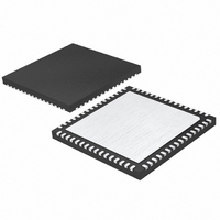
LTC2242IUP-10#PBF Linear Technology, LTC2242IUP-10#PBF Datasheet - Page 3

LTC2242IUP-10#PBF
Manufacturer Part Number
LTC2242IUP-10#PBF
Description
IC ADC 10BIT 250MSPS 64-QFN
Manufacturer
Linear Technology
Datasheet
1.LTC2242CUP-10PBF.pdf
(28 pages)
Specifications of LTC2242IUP-10#PBF
Number Of Bits
10
Sampling Rate (per Second)
250M
Data Interface
Parallel
Number Of Converters
1
Power Dissipation (max)
975mW
Voltage Supply Source
Single Supply
Operating Temperature
-40°C ~ 85°C
Mounting Type
Surface Mount
Package / Case
64-WFQFN, Exposed Pad
Lead Free Status / RoHS Status
Lead free / RoHS Compliant
ANALOG INPUT
DYNAMIC ACCURACY
CONVERTER CHARACTERISTICS
temperature range, otherwise specifi cations are at T
PARAMETER
Offset Drift
Full-Scale Drift
Transition Noise
specifi cations are at T
otherwise specifi cations are at T
SYMBOL
SNR
SFDR
S/(N+D)
IMD
SYMBOL
V
V
I
I
I
I
t
t
IN
SENSE
MODE
LVDS
AP
JITTER
IN
IN, CM
PARAMETER
Analog Input Range (A
Analog Input Common Mode (A
Analog Input Leakage Current
SENSE Input Leakage
MODE Pin Pull-Down Current to GND
LVDS Pin Pull-Down Current to GND
Sample and Hold Acquisition Delay Time
Sample and Hold Acquisition Delay Time Jitter
Full Power Bandwidth
PARAMETER
Signal-to-Noise Ratio (Note 10)
Spurious Free Dynamic Range
2nd or 3rd Harmonic
(Note 11)
Spurious Free Dynamic Range
4th Harmonic or Higher
(Note 11)
Signal-to-Noise Plus
Distortion Ratio
(Note 12)
Intermodulation Distortion
A
= 25°C. (Note 4)
The
A
IN
= 25°C. A
+
●
– A
denotes the specifi cations which apply over the full operating temperature range, otherwise
IN
–
IN
)
+
The
IN
+ A
= –1dBFS. (Note 4)
IN
●
–
CONDITIONS
Internal Reference
External Reference
SENSE = 1V
denotes the specifi cations which apply over the full operating temperature range,
)/2
A
= 25°C. (Note 4)
CONDITIONS
10MHz Input
70MHz Input
140MHz Input
240MHz Input
10MHz Input
70MHz Input
140MHz Input
240MHz Input
10MHz Input
70MHz Input
140MHz Input
240MHz Input
10MHz Input
70MHz Input
140MHz Input
240MHz Input
f
IN1
The
CONDITIONS
= 135MHz, f
2.375V < V
Differential Input (Note 7)
0 < A
0V < SENSE < 1V
Figure 8 Test Circuit
l
IN
denotes the specifi cations which apply over the full operating
+
, A
IN
DD
IN2
–
< 2.625V (Note 7)
< V
= 140MHz
DD
l
l
l
l
●
●
●
●
MIN
59.2
58.2
MIN
1.2
63
71
–1
–1
MIN
LTC2242-10
±0.5 to ±1
60.6
60.5
60.5
60.4
60.4
60.4
60.3
60.2
TYP
1200
78
75
74
73
85
85
85
85
81
1.25
TYP
0.18
TYP
±10
±60
±45
0.4
95
7
7
MAX
MAX
MAX
1.3
1
1
LSB
224210fc
ppm/C
ppm/C
UNITS
UNITS
UNITS
fs
3
μV/C
MHz
RMS
RMS
dBc
μA
μA
μA
μA
ns
dB
dB
dB
dB
dB
dB
dB
dB
dB
dB
dB
dB
dB
dB
dB
dB
V
V


