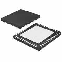
LTC2206IUK-14#PBF Linear Technology, LTC2206IUK-14#PBF Datasheet - Page 25

LTC2206IUK-14#PBF
Manufacturer Part Number
LTC2206IUK-14#PBF
Description
IC ADC 14BIT 80MSPS 48-QFN
Manufacturer
Linear Technology
Datasheet
1.LTC2206CUK-14PBF.pdf
(32 pages)
Specifications of LTC2206IUK-14#PBF
Number Of Bits
14
Sampling Rate (per Second)
80M
Data Interface
Parallel
Number Of Converters
1
Power Dissipation (max)
875mW
Voltage Supply Source
Single Supply
Operating Temperature
-40°C ~ 85°C
Mounting Type
Surface Mount
Package / Case
48-WFQFN, Exposed Pad
Lead Free Status / RoHS Status
Lead free / RoHS Compliant
Available stocks
Company
Part Number
Manufacturer
Quantity
Price
APPLICATIONS INFORMATION
As shown in Figure 14, the output of the sample-and-hold
amplifi er is summed with the output of a dither DAC. The
dither DAC is driven by a long sequence pseudo-random
number generator; the random number fed to the dither
DAC is also subtracted from the ADC result. If the dither
DAC is precisely calibrated to the ADC, very little of the
dither signal will be seen at the output. The dither signal
that does leak through will appear as white noise. The dither
DAC is calibrated to result in less than 0.5dB elevation in
the noise fl oor of the ADC, as compared to the noise fl oor
with dither off.
Grounding and Bypassing
The LTC2207-14/LTC2206-14 require a printed circuit board
with a clean unbroken ground plane; a multilayer board
with an internal ground plane is recommended. The pinout
of the LTC2207-14/LTC2206-14 has been optimized for a
fl owthrough layout so that the interaction between inputs
and digital outputs is minimized. Layout for the printed
circuit board should ensure that digital and analog signal
lines are separated as much as possible. In particular, care
ANALOG
INPUT
AIN
AIN
+
–
Figure 14. Functional Equivalent Block Diagram of Internal Dither Circuit
CLOCK/DUTY
ENC
CONTROL
AMP
S/H
CYCLE
+
ENC
–
PRECISION
PIPELINED
ADC CORE
14-BIT
DAC
should be taken not to run any digital track alongside an
analog signal track or underneath the ADC.
High quality ceramic bypass capacitors should be used
at the V
be located as close to the pins as possible. The traces
connecting the pins and bypass capacitors must be kept
short and should be made as wide as possible.
The LTC2207-14/LTC2206-14 differential inputs should run
parallel and close to each other. The input traces should
be as short as possible to minimize capacitance and to
minimize noise pickup.
Heat Transfer
Most of the heat generated by the LTC2207-14/LTC2206-
14 is transferred from the die through the bottom-side
exposed pad. For good electrical and thermal performance,
the exposed pad must be soldered to a large grounded
pad on the PC board. It is critical that the exposed pad
and all ground pins are connected to a ground plane of
suffi cient area with as many vias as possible.
SUMMATION
LTC2207-14/LTC2206-14
DD,
DIGITAL
V
HIGH = DITHER ON, LOW = DITHER OFF
CM
, and OV
LTC2207-14/LTC2206-14
PSEUDO-RANDOM
MULTIBIT DEEP
DITHER ENABLE
GENERATOR
NUMBER
DRIVERS
OUTPUT
DITH
DD
pins. Bypass capacitors must
2207614 F14
CLKOUT
D13
D0
OF
•
•
•
220714614fc
25


