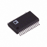
AD9200ARSRL Analog Devices Inc, AD9200ARSRL Datasheet - Page 6

AD9200ARSRL
Manufacturer Part Number
AD9200ARSRL
Description
IC ADC 10BIT CMOS 20MSPS 28-SSOP
Manufacturer
Analog Devices Inc
Datasheet
1.AD9200ARSZRL.pdf
(24 pages)
Specifications of AD9200ARSRL
Rohs Status
RoHS non-compliant
Number Of Bits
10
Sampling Rate (per Second)
20M
Data Interface
Parallel
Number Of Converters
9
Power Dissipation (max)
100mW
Voltage Supply Source
Single Supply
Operating Temperature
-40°C ~ 85°C
Mounting Type
Surface Mount
Package / Case
28-SSOP (0.200", 5.30mm Width)
AD9200
DEFINITIONS OF SPECIFICATIONS
Integral Nonlinearity (INL)
Integral nonlinearity refers to the deviation of each individual
code from a line drawn from “zero” through “full scale”. The
point used as “zero” occurs 1/2 LSB before the first code transi-
tion. “Full scale” is defined as a level 1 1/2 LSB beyond the last
code transition. The deviation is measured from the center of
each particular code to the true straight line.
Differential Nonlinearity (DNL, No Missing Codes)
An ideal ADC exhibits code transitions that are exactly 1 LSB
apart. DNL is the deviation from this ideal value. It is often
specified in terms of the resolution for which no missing codes
(NMC) are guaranteed.
Typical Characterization Curves
–0.5
–1.0
–0.5
–1.0
1.0
0.5
1.0
0.5
0
0
0
0
128
128
Figure 3. Typical DNL
Figure 4. Typical INL
256
256
384
384
CODE OFFSET
CODE OFFSET
512
512
640
640
768
768
896
896
(AVDD = +3 V, DRVDD = +3 V, F
Span from 0.5 V to 2.5 V, External Reference, unless otherwise noted)
1024
1024
–6–
Offset Error
The first transition should occur at a level 1 LSB above “zero.”
Offset is defined as the deviation of the actual first code transi-
tion from that point.
Gain Error
The first code transition should occur for an analog value 1 LSB
above nominal negative full scale. The last transition should
occur for an analog value 1 LSB below the nominal positive full
scale. Gain error is the deviation of the actual difference be-
tween first and last code transitions and the ideal difference
between the first and last code transitions.
Pipeline Delay (Latency)
The number of clock cycles between conversion initiation and
the associated output data being made available. New output
data is provided every rising edge.
1.00E+05
1.00E+05
60
55
50
45
40
35
30
25
20
60
55
50
45
40
35
30
25
20
S
Figure 6. SINAD vs. Input Frequency
Figure 5. SNR vs. Input Frequency
= 20 MHz (50% Duty Cycle), MODE = AVDD, 2 V Input
1.00E+06
1.00E+06
INPUT FREQUENCY – Hz
INPUT FREQUENCY – Hz
–20.0 AMPLITUDE
–20.0 AMPLITUDE
–0.5 AMPLITUDE
–6.0 AMPLITUDE
–0.5 AMPLITUDE
–6.0 AMPLITUDE
1.00E+07
1.00E+07
1.00E+08
1.00E+08
REV. E


