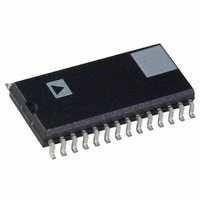
AD7708BR Analog Devices Inc, AD7708BR Datasheet - Page 3

AD7708BR
Manufacturer Part Number
AD7708BR
Description
IC ADC 16BIT R-R 8/10CH 28-SOIC
Manufacturer
Analog Devices Inc
Datasheet
1.AD7708BRUZ-REEL.pdf
(44 pages)
Specifications of AD7708BR
Mounting Type
Surface Mount
Rohs Status
RoHS non-compliant
Number Of Bits
16
Sampling Rate (per Second)
1.37k
Data Interface
DSP, MICROWIRE™, QSPI™, Serial, SPI™
Number Of Converters
1
Power Dissipation (max)
3.84mW
Voltage Supply Source
Analog and Digital
Operating Temperature
-40°C ~ 85°C
Package / Case
28-SOIC (0.300", 7.50mm Width)
Peak Reflow Compatible (260 C)
No
No. Of Bits
16 Bit
Leaded Process Compatible
No
Features
Analog Front End For Low Frequency Measurement
No. Of Channels
8
For Use With
EVAL-AD7708EBZ - BOARD EVAL FOR AD7708
Lead Free Status / RoHS Status
Contains lead / RoHS non-compliant
Available stocks
Company
Part Number
Manufacturer
Quantity
Price
Part Number:
AD7708BRU
Manufacturer:
ADI/亚德诺
Quantity:
20 000
Part Number:
AD7708BRUZ
Manufacturer:
ADI/亚德诺
Quantity:
20 000
Part Number:
AD7708BRUZ-REEL
Manufacturer:
ADI/亚德诺
Quantity:
20 000
Company:
Part Number:
AD7708BRUZ-REEL7
Manufacturer:
TE
Quantity:
7 600
Part Number:
AD7708BRZ
Manufacturer:
ADI/亚德诺
Quantity:
20 000
AD7718 SPECIFICATIONS
REFIN(+) = 2.5 V; REFIN(–) = AGND; AGND = DGND = 0 V; XTAL1/XTAL2 = 32.768 kHz Crystal Input Buffer Enabled. All specifications T
T
Parameter
AD7718 (CHOP DISABLED)
ANALOG INPUTS
REFERENCE INPUTS (REFIN1 AND REFIN2)
MAX
Output Update Rate
No Missing Codes
Resolution
Output Noise and Update Rates
Integral Nonlinearity
Offset Error
Offset Error Drift vs. Temp
Full-Scale Error
Gain Drift vs. Temp
Negative Full-Scale Error
Differential Input Full-Scale Voltage
Absolute AIN Voltage Limits
Absolute AINCOM Voltage Limits
Analog Input Current
AINCOM Input Current
Normal-Mode Rejection
Common-Mode Rejection
REFIN(+) to REFIN(–) Voltage
REFIN(+) to REFIN(–) Range
REFIN Common-Mode Range
Reference DC Input Current
Reference DC Input Current Drift
Normal-Mode Rejection
Common-Mode Rejection
unless otherwise noted.)
DC Input Current
DC Bias Current Drift
DC Input Current
DC Bias Current Drift
@ 50 Hz
@ 60 Hz
@ DC
@ 50 Hz
@ 60 Hz
@ 50 Hz
@ 60 Hz
@ DC
@ 50 Hz
@ 60 Hz
3
3
2
4
2
2
2
2
4
2
B Grade
16.06
1.365
24
13
18
See Tables in
ADC Description
± 10
Table VII
± 200
± 10
± 0.5
± 0.003
± 1.024 × REFIN/GAIN V nom
AGND + 100 mV
AV
AGND – 30 mV
AV
± 1
± 5
± 125
± 2
100
100
90
100
100
2.5
1
AV
AGND – 30 mV
AV
0.5
± 0.1
100
100
100
100
100
1
DD
DD
DD
DD
(AV
– 100 mV
+ 30 mV
+ 30 mV
DD
= 2.7 V to 3.6 V or 4.75 V to 5.25 V, DV
Unit
Hz min
kHz max
Bits min
Bits p-p
Bits p-p
ppm of FSR max
µV typ
nV/°C typ
µV typ
ppm/°C typ
% FSR max
V min
V max
V min
V max
nA max
pA/°C typ
nA/V typ
pA/V/°C typ
dB min
dB min
dB min
dB typ
dB typ
V nom
V min
V max
V min
V max
µA/V typ
nA/V/°C typ
dB min
dB min
dB typ
dB typ
dB typ
Test Conditions
CHOP = 1
± 20 mV Range, SF = 69
± 2.56 V Range, SF = 69
2 ppm Typical
Offset Error is in the order of the noise for the
programmed gain and update rate following a
calibration
REFIN Refers to Both REFIN1 and
REFIN2. REFIN = REFIN(+) –REFIN(–)
GAIN = 1 to 128
AIN1–AIN10 and AINCOM with
NEGBUF = 1
NEGBUF = 0
AIN1–AIN10 and AINCOM with NEGBUF = 1
NEGBUF = 0
± 2.56 V Range
50 Hz ± 1 Hz, SF Word = 82
60 Hz ± 1 Hz, SF Word = 68
100 dB typ, Analog Input = 1 V,
Input Range = ± 2.56 V
110 dB typ on ± 20 mV Range
50 Hz ± 1 Hz, SF Word = 82
60 Hz ± 1 Hz, SF Word = 68
REFIN Refers to Both REFIN1 and REFIN2
50 Hz ± 1 Hz, SF Word = 82
60 Hz ± 1 Hz, SF Word = 68
Input Range = ± 2.56 V
Analog Input = 1 V. Input Range = ± 2.56 V
DD
= 2.7 V to 3.6 V or 4.75 V to 5.25 V,
AD7708/AD7718
MIN
to


