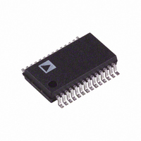
AD9051BRS Analog Devices Inc, AD9051BRS Datasheet - Page 9

AD9051BRS
Manufacturer Part Number
AD9051BRS
Description
IC ADC 10BIT 60MSPS 28-SSOP
Manufacturer
Analog Devices Inc
Specifications of AD9051BRS
Mounting Type
Surface Mount
Package / Case
28-SSOP (0.200", 5.30mm Width)
Rohs Status
RoHS non-compliant
Number Of Bits
10
Sampling Rate (per Second)
60M
Data Interface
Parallel
Number Of Converters
3
Power Dissipation (max)
315mW
Voltage Supply Source
Analog and Digital
Operating Temperature
-40°C ~ 85°C
Peak Reflow Compatible (260 C)
No
No. Of Bits
10 Bit
Leaded Process Compatible
No
No. Of Channels
2
Interface Type
Parallel
Number Of Elements
1
Resolution
10Bit
Architecture
Pipelined
Sample Rate
60MSPS
Input Polarity
Unipolar
Input Type
Voltage
Rated Input Volt
±0.625V
Differential Input
Yes
Power Supply Requirement
Single
Single Supply Voltage (typ)
5V
Dual Supply Voltage (typ)
Not RequiredV
Dual Supply Voltage (min)
Not RequiredV
Dual Supply Voltage (max)
Not RequiredV
Power Dissipation
315mW
Differential Linearity Error
1.5LSB
Integral Nonlinearity Error
1.5LSB
Operating Temp Range
-40C to 85C
Operating Temperature Classification
Industrial
Mounting
Surface Mount
Pin Count
28
Package Type
SSOP
Lead Free Status / Rohs Status
Not Compliant
Available stocks
Company
Part Number
Manufacturer
Quantity
Price
Company:
Part Number:
AD9051BRS-2V
Manufacturer:
AD
Quantity:
340
Part Number:
AD9051BRS-2V
Manufacturer:
ADI/亚德诺
Quantity:
20 000
Part Number:
AD9051BRSZ
Manufacturer:
ADI/亚德诺
Quantity:
20 000
Company:
Part Number:
AD9051BRSZ-2V
Manufacturer:
IML
Quantity:
3 000
Company:
Part Number:
AD9051BRSZRL
Manufacturer:
TOSHIBA
Quantity:
5 600
Part Number:
AD9051BRSZRL
Manufacturer:
ADI/亚德诺
Quantity:
20 000
THEORY OF OPERATION
Refer to the block diagram on the front page.
The AD9051 employs a subranging architecture with digital
error correction. This combination of design techniques ensures
true 10-bit accuracy at the digital outputs of the converter.
At the input, the analog signal is buffered by a high speed
differential buffer and applied to a track-and-hold (T/H) that
holds the analog value present when the unit is strobed with
an ENCODE command. The conversion process begins on the
rising edge of this pulse. The two stage architecture completes a
coarse and then a fine conversion of the T/H output signal.
Error correction and decode logic correct and align data from
the two conversions and present the result as a 10-bit parallel
digital word. Output data are strobed on the rising edge of the
ENCODE command. The subranging architecture results in
five pipeline delays for the output data. Refer to the AD9051
Timing Diagram.
USING THE AD9051
3 V System
The digital input and outputs of the AD9051 can be easily
configured to directly interface to 3 V logic systems. The encode
input (Pin 13) is TTL compatible with a logic threshold of
1.5 V. This input is actually a CMOS stage (refer to Equivalent
Encode Input Stage) with a TTL threshold, allowing operation
with TTL, CMOS and 3 V CMOS logic families. Using 3 V
CMOS logic allows the user to drive the encode directly without
the need to translate to 5 V. This saves the user power and
board space. As with all high speed data converters, the clock
signal must be clean and jitter free to prevent the degradation of
dynamic performance.
The AD9051 outputs can also directly interface to 3 V logic
systems. The digital outputs are standard CMOS stages (refer
to AD9051 Output Stage) with isolated supply pins (Pins 20,
22 V
output levels vary respectively. By connecting Pins 20 and 22 to
the 3 V logic supply, the AD9051 will supply 3 V output
levels. Care should be taken to filter and isolate the output
supply of the AD9051 as noise could be coupled into the
ADC, limiting performance.
Analog Input
The analog input of the AD9051 is a differential input buffer
(refer to AD9051 Equivalent Analog Input). The differential
inputs are internally biased at 2.5 V, obviating the need for
external biasing. Excellent performance is achieved whether the
analog inputs are driven single-endedly or differentially (for
best dynamic performance, impedances at AIN and AINB
should match).
Figure 3 shows typical connections for the analog inputs when
using the AD9051 in a dc-coupled system with single-ended
signals. All components are powered from a single 5 V supply.
The AD820 is used to offset the ground referenced input signal
to the level required by the AD9051.
AC coupling of the analog inputs of the AD9051 is easily
accomplished. Figure 4 shows capacitive coupling of a single-
ended signal while Figure 5 shows transformer coupling
differentially into the AD9051.
DD
). By varying the voltage on the V
DD
pins, the digital
The AD830 provides a unique method of providing dc level
shift for the analog input. Using the AD830 allows a great deal
of flexibility for adjusting offset and gain. Figure 6 shows the
AD830 configured to drive the AD9051. The offset is provided
by the internal biasing of the AD9051 differential input (Pin 9).
For more information regarding the AD830, see the AD830
data sheet.
–0.625V
+0.625V
–0.625V
+0.625V
V
TO
V
TO
IN
IN
–0.625V
+0.625V
–0.625V
+0.625V
V
TO
V
IN
TO
IN
140
0.1 F
1k
140
140
140
+5V
–5V
2
3
4
1
1k
AD830
AD9631
140
140
5V
+5V
–5V
+15V
–5V
AD820
AD9631
AD9631
0.1 F
7
5V
50
0.1 F
0.1 F
0.1 F
T1-1T
9
10
10
9
10
9
0.1 F
AD9051
10
AD9051
AD9051
AD9051
9
+5V
5V
AD9051
5V
5V


