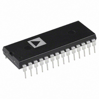
AD7862ANZ-10 Analog Devices Inc, AD7862ANZ-10 Datasheet - Page 13

AD7862ANZ-10
Manufacturer Part Number
AD7862ANZ-10
Description
IC ADC 12BIT DUAL 250KSPS 28DIP
Manufacturer
Analog Devices Inc
Datasheet
1.AD7862ARZ-10.pdf
(16 pages)
Specifications of AD7862ANZ-10
Data Interface
Parallel
Number Of Bits
12
Sampling Rate (per Second)
250k
Number Of Converters
2
Power Dissipation (max)
75mW
Voltage Supply Source
Analog and Digital
Operating Temperature
-40°C ~ 85°C
Mounting Type
Through Hole
Package / Case
28-DIP (0.600", 15.24mm)
Resolution (bits)
12bit
Sampling Rate
250kSPS
Input Channel Type
Single Ended
Supply Voltage Range - Analog
4.75V To 5.25V
Supply Current
15mA
Digital Ic Case Style
DIP
Lead Free Status / RoHS Status
Lead free / RoHS Compliant
Available stocks
Company
Part Number
Manufacturer
Quantity
Price
Part Number:
AD7862ANZ-10
Manufacturer:
ADI/亚德诺
Quantity:
20 000
MICROPROCESSOR INTERFACING
The AD7862 high speed bus timing allows direct interfacing to
DSP processors as well as modern 16-bit microprocessors.
Suitable microprocessor interfaces are shown in Figures 14
through 18.
AD7862–ADSP-2100 Interface
Figure 14 shows an interface between the AD7862 and the
ADSP-2100. The CONVST signal can be supplied from the
ADSP-2100 or from an external source. The AD7862 BUSY
line provides an interrupt to the ADSP-2100 when conversion is
completed on all four channels. The four conversion results can
then be read from the AD7862 using four successive reads to
the same memory address. The following instruction reads one
of the four results (this instruction is repeated four times to read
all four results in sequence):
where MR0 is the ADSP-2100 MR0 register, and ADC is the
AD7862 address.
AD7862–ADSP-2101/ADSP-2102 INTERFACE
The interface outlined in Figure 14 also forms the basis for an
interface between the AD7862 and the ADSP-2101/ADSP-2102.
The READ line of the ADSP-2101/ADSP-2102 is labeled RD.
In this interface, the RD pulse width of the processor can be
programmed using the Data Memory Wait State Control Register.
The instruction used to read one of the four results is outlined
for the ADSP-2100.
AD7862–TMS32010 Interface
An interface between the AD7862 and the TMS32010 is shown
in Figure 15. Once again, the CONVST signal can be supplied
from the TMS32010 or from an external source, and the
TMS32010 is interrupted when both conversions have been
completed. The following instruction is used to read the conver-
sion results from the AD7862:
where D is Data Memory address, and ADC is the AD7862
address.
REV. 0
(ADSP-2101/
ADSP-2102)
ADSP-2100
Figure 14. AD7862–ADSP-2100 Interface
DMRD (RD)
DMD15
DMA13
DMA0
DMD0
IRQn
DMS
* ADDITIONAL PINS OMITTED FOR CLARITY
MR0 = DM(ADC)
ADDRESS BUS
IN D,ADC
DATA BUS
EN
DECODE
ADDR
A0
BUSY
CS
RD
DB11
DB0
AD7862*
OPTIONAL
CONVST
–13–
AD7862–TMS320C25 Interface
Figure 16 shows an interface between the AD7862 and the
TMS320C25. As with the two previous interfaces, conversion
can be initiated from the TMS320C25 or from an external
source, and the processor is interrupted when the conversion
sequence is completed. The TMS320C25 does not have a
separate RD output to drive the AD7862 RD input directly.
This has to be generated from the processor STRB and R/W
outputs with the addition of some logic gates. The RD signal is
OR-gated with the MSC signal to provide the one WAIT state
required in the read cycle for correct interface timing. Conver-
sion results are read from the AD7862 using the following
instruction:
where D is Data Memory address and ADC is the AD7862
address.
TMS320C25
Figure 16. AD7862–TMS320C25 Interface
TMS32010
Figure 15. AD7862–TMS32010 Interface
READY
STRB
MEN
DEN
PA0
INTn
MSC
D15
PA2
A15
R/W
INT
D15
D0
A0
D0
IS
* ADDITIONAL PINS OMITTED FOR CLARITY
*ADDITIONAL PINS OMITTED FOR CLARITY
ADDRESS BUS
IN D,ADC
ADDRESS BUS
DATA BUS
EN
DECODE
EN
ADDR
DECODE
ADDR
DATA BUS
OPTIONAL
OPTIONAL
CONVST
A0
BUSY
CS
RD
DB11
DB0
BUSY
DB11
DB0
CONVST
A0
CS
RD
AD7862*
AD7862*
AD7862


