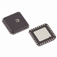
AD9237BCPZ-65 Analog Devices Inc, AD9237BCPZ-65 Datasheet - Page 3

AD9237BCPZ-65
Manufacturer Part Number
AD9237BCPZ-65
Description
IC ADC 12BIT SGL 65MSPS 32LFCSP
Manufacturer
Analog Devices Inc
Specifications of AD9237BCPZ-65
Data Interface
Parallel
Number Of Bits
12
Sampling Rate (per Second)
65M
Number Of Converters
3
Power Dissipation (max)
190mW
Voltage Supply Source
Single Supply
Operating Temperature
-40°C ~ 85°C
Mounting Type
Surface Mount
Package / Case
32-VFQFN, CSP Exposed Pad
Resolution (bits)
12bit
Input Channel Type
Differential
Supply Voltage Range - Analogue
2.7V To 3.6V
Supply Voltage Range - Digital
2.25V To 3.6V
Supply Current
64.5mA
Sampling Rate
65MSPS
Rohs Compliant
Yes
Number Of Elements
1
Resolution
12Bit
Architecture
Pipelined
Sample Rate
65MSPS
Input Polarity
Unipolar
Input Type
Voltage
Rated Input Volt
±0.5/±1/±2V
Differential Input
Yes
Power Supply Requirement
Single
Single Supply Voltage (typ)
3V
Single Supply Voltage (min)
2.7V
Single Supply Voltage (max)
3.6V
Dual Supply Voltage (typ)
Not RequiredV
Dual Supply Voltage (min)
Not RequiredV
Dual Supply Voltage (max)
Not RequiredV
Power Dissipation
270mW
Differential Linearity Error
±1.25LSB
Integral Nonlinearity Error
±2LSB
Operating Temp Range
-40C to 85C
Operating Temperature Classification
Industrial
Mounting
Surface Mount
Pin Count
32
Package Type
LFCSP EP
Lead Free Status / RoHS Status
Lead free / RoHS Compliant
Lead Free Status / RoHS Status
Lead free / RoHS Compliant, Lead free / RoHS Compliant
Available stocks
Company
Part Number
Manufacturer
Quantity
Price
Company:
Part Number:
AD9237BCPZ-65
Manufacturer:
CREE
Quantity:
101
SPECIFICATIONS
DC SPECIFICATIONS
AVDD = 3 V, DRVDD = 2.5 V, maximum sample rate, 2 V p-p differential input, −0.5 dBFS input, 1.0 V internal reference, T
unless otherwise noted.
Table 1.
Parameter
RESOLUTION
ACCURACY
TEMPERATURE DRIFT
INTERNAL VOLTAGE REFERENCE
INPUT REFERRED NOISE
ANALOG INPUT
POWER SUPPLIES
POWER CONSUMPTION
1
2
3
4
Gain error and gain temperature coefficient are based on the ADC only (with a fixed 1.0 V external reference).
Measured at maximum clock rate, f
Input capacitance refers to the effective capacitance between one differential input pin and AGND. Refer to
Measured with dc input at maximum clock rate.
No Missing Codes Guaranteed
Offset Error
Gain Error
Differential Nonlinearity (DNL)
Integral Nonlinearity (INL)
Offset Error
Gain Error
Output Voltage Error (1 V Mode)
Load Regulation @ 1.0 mA
Output Voltage Error (0.5 V Mode)
Load Regulation @ 0.5 mA
Reference Input Resistance
VREF = 0.5 V
VREF = 1.0 V
Input Span
Input Capacitance
Supply Voltages
Supply Current
PSRR
DC Input
Sine Wave Input
Power-Down Mode
Standby Power
VREF = 0.5 V; MODE2 = 0 V
VREF = 1.0 V; MODE2 = 0 V
VREF = 0.5 V; MODE2 = AVDD
VREF = 1.0 V; MODE2 = AVDD
AVDD
DRVDD
IAVDD
IDRVDD
2
4
1
1
2
2
3
2
IN
= 2.4 MHz, full-scale sine wave, with approximately 5 pF loading on each output bit.
2
Min
12
12
2.7
2.25
AD9237BCP-20
Typ
±1.30
±0.70
±0.70
±0.90
±2
±12
±5
0.8
±2.5
0.1
7
1.35
0.70
7
3.0
2.5
30.5
3.0
±0.01
85
100
1
20
Rev. A | Page 3 of 24
Max
±1.95
±2.10
±0.95
±1.35
±25
1
2
2
4
3.6
3.6
120
Min
12
12
2.7
2.25
AD9237BCP-40
Typ
±1.30
±0.75
±0.70
±0.90
±2
±12
±5
0.8
±2.5
0.1
7
1.35
0.70
7
3.0
2.5
45.5
4.5
±0.01
135
150
1
20
Max
±1.95
±2.10
±0.95
±1.35
±25
1
2
2
4
3.6
3.6
180
Figure 4
for the equivalent analog input structure.
Min
12
12
−1.00
2.7
2.25
AD9237BCP-65
1.35
0.70
Typ
±1.30
±1.05
±0.70
±0.90
±2
±12
±5
0.8
±2.5
0.1
7
7
3.0
2.5
64.5
5.5
±0.01
190
210
1
20
Max
±1.95
±2.25
+1.25
±2.00
±25
1
2
2
4
3.6
3.6
270
MIN
AD9237
to T
LSB rms
LSB rms
Unit
Bits
Bits
% FSR
% FSR
LSB
LSB
ppm/°C
ppm/°C
mV
mV
mV
mV
kΩ
V p-p
V p-p
V p-p
V p-p
pF
V
V
mA
mA
% FSR
mW
mW
mW
mW
MAX
,


