AD7861AP Analog Devices Inc, AD7861AP Datasheet - Page 5
AD7861AP
Manufacturer Part Number
AD7861AP
Description
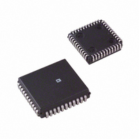
IC ADC 11BIT 4CH 44-PLCC
Manufacturer
Analog Devices Inc
Datasheet
1.AD7861APZ.pdf
(6 pages)
Specifications of AD7861AP
Rohs Status
RoHS non-compliant
Number Of Bits
11
Sampling Rate (per Second)
28.6k
Data Interface
Parallel
Number Of Converters
1
Power Dissipation (max)
50mW
Voltage Supply Source
Single Supply
Operating Temperature
-40°C ~ 85°C
Mounting Type
Surface Mount
Package / Case
44-PLCC
Available stocks
Company
Part Number
Manufacturer
Quantity
Price
Company:

Part Number:
AD7861AP
Manufacturer:
Analog Devices Inc.
Quantity:
245
Part Number:
AD7861AP
Manufacturer:
ADI/亚德诺
Quantity:
20 000
Company:
Part Number:
AD7861APZ
Manufacturer:
Analog Devices Inc
Quantity:
10 000


REV. B
ANALOG INPUT BLOCK
The AD7861 is an 11-bit resolution, successive approximation
analog-to-digital (A/D) converter with twos complement output
data format. The analog input range is 0 V–5 V with a 2.5 V
reference as defined by the reference input pin (REFIN). The
AD7861 has an internal 2.5 V ± 5% reference, which is utilized
by connecting the reference output pin (REFOUT) to the
REFIN pin.
The A/D conversion time is determined by the system clock
frequency, which can range from 6.25 MHz to 12.5 MHz.
Forty clock cycles are required to complete each conversion.
There is a 4-channel simultaneous sample and hold amplifier
(SHA) at the AD7861 input stage. This allows up to 4 channels to
be simultaneously held and sequentially digitized. The SHA
acquisition time is 20 clock cycles and is independent of the
number of channels sampled.
The minimum throughput time can be calculated as follows:
where t
time, n = # channels, t
(40 clock cycles).
A/D conversions are initiated by an external analog sample
clock pin (CONVST).
The CONVST input can be run asynchronous to the AD7861
system clock. When CONVST is run asynchronous from CLK,
the falling edge of CLK subsequent to CONVST high initiates
the conversion.
BUSY
The AD7861 BUSY pin goes low at the start of conversion, and
remains low for 40 clock cycles per channel. When BUSY goes
high, this indicates that the output data buffers have been
updated. Data from the previous conversion can be read up to
(n × 40 – 1) clock cycles after the start of conversion (n =
number of channels converted). Refer to Figure 3.
CHANNEL SELECTION
Determining which channels are converted is dependent on the
settings of M0 and M1. The available channel combinations are:
M1
0
0
1
1
CONVST
BUSY
DATA
CLK
AA
= analog acquisition time, t
M0
0
1
0
1
Figure 3. Busy Pulse Timing
t
(n x 40 –1) CLOCK CYCLES
OLD DATA VALID
t
= 1 CLOCK CYCLE
AA
CONV
= t
SHA
= conversion time per channel
Channels Converted
VIN2, VIN3
VIN2, VIN3, AUX
VIN1, VIN2, VIN3
VIN1, VIN2, VIN3, AUX
+ (n × t
SHA
CONV
t
= (n x 40 –1) CLOCK CYCLES
= SHA acquisition
t
NEW DATA VALID
= n x 40 CLOCK CYCLES
)
–5–
The user must select which channels to convert using M0/M1, a
minimum of two clock cycles before the start of conversion.
The AD7861 provides 4 auxiliary input channels which can be
individually multiplexed into the auxiliary ADC channel. Pins S0/
S1 are used to multiplex these auxiliary channels according to the
following table. It is important to note that the ADC performs a
series of conversions based on the input voltage on each pin
(including the AUX pin) at the start of the CONVST conversion
pulse. The user must select the auxiliary channel using S0/S1
a minimum of two clock cycles before the start of the conversion
sequence.
DIGITAL INTERFACE
The AD7861 is designed to interface with the ADSP-21xx
family of DSPs. The 12-bit parallel interface can also be used
with other DSPs and microcontrollers.
The 11-bit A/D conversion output occupies the 11 most
significant bits of the 12-bit interface. The LSB (Data Bit 0) is
tied low.
REGISTER BASED INPUT/OUTPUT
To facilitate integration into most designs, a register based
input/output structure is provided. These registers can be
memory mapped into the user’s system along with other
memory mapped peripherals.
REGISTER ADDRESSING
Two address lines (A0 through A1) are used in conjunction with
control lines (CS, RD) to select registers VIN1, VIN2, VIN3, or
AUX. These control lines are active low. Timing and logical
sense is as for the ADSP-2100 family.
REGISTER LISTING
The output of each channel is stored in its respective register.
The symbolic names and address locations are listed in the
following table.
Name
VIN1
VIN2
VIN3
AUX
S1
0
0
1
1
Pin
CS
RD
A1
0
0
1
1
Function
Enables the AD7861 Register Interface
Places the Internal Register on the Data Bus
A0
0
1
0
1
S0
0
1
0
1
Register Function
A/D Conversion Result Channel VIN1
A/D Conversion Result Channel VIN2
A/D Conversion Result Channel VIN3
A/D Conversion Result Channel AUX
Channel Selected
AUX0
AUX1
AUX2
AUX3
AD7861
Related parts for AD7861AP
Image
Part Number
Description
Manufacturer
Datasheet
Request
R

Part Number:
Description:
±1.7g Dual-Axis IMEMS Accelerometer Evaluation Board
Manufacturer:
Analog Devices Inc
Datasheet:

Part Number:
Description:
Inertial Sensor Evaluation System
Manufacturer:
Analog Devices Inc
Datasheet:
Part Number:
Description:
Manufacturer:
Analog Devices Inc
Datasheet:
Part Number:
Description:
Manufacturer:
Analog Devices Inc
Datasheet:
Part Number:
Description:
Manufacturer:
Analog Devices Inc
Datasheet:
Part Number:
Description:
Manufacturer:
Analog Devices Inc
Datasheet:
Part Number:
Description:
Manufacturer:
Analog Devices Inc
Datasheet:
Part Number:
Description:
Manufacturer:
Analog Devices Inc
Datasheet:
Part Number:
Description:
Manufacturer:
Analog Devices Inc
Datasheet:
Part Number:
Description:
Manufacturer:
Analog Devices Inc
Datasheet:
Part Number:
Description:
Manufacturer:
Analog Devices Inc
Datasheet:
Part Number:
Description:
Manufacturer:
Analog Devices Inc
Datasheet:
Part Number:
Description:
Manufacturer:
Analog Devices Inc
Datasheet: