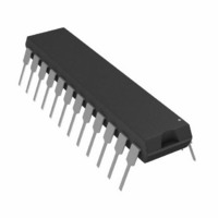
AD7711AN Analog Devices Inc, AD7711AN Datasheet - Page 23

AD7711AN
Manufacturer Part Number
AD7711AN
Description
IC ADC 24BIT RTD I SOURCE 24-DIP
Manufacturer
Analog Devices Inc
Datasheet
1.AD7711ARZ.pdf
(28 pages)
Specifications of AD7711AN
Mounting Type
Through Hole
Rohs Status
RoHS non-compliant
Number Of Bits
24
Sampling Rate (per Second)
1.03k
Data Interface
Serial
Number Of Converters
1
Power Dissipation (max)
45mW
Voltage Supply Source
Analog and Digital, Dual ±
Operating Temperature
-40°C ~ 80°C
Package / Case
24-DIP (0.300", 7.62mm)
No. Of Channels
1
Peak Reflow Compatible (260 C)
No
No. Of Bits
24 Bit
Leaded Process Compatible
No
Features
Signal Conditioning
Compl. Anal. Front-end
RoHS Compliant
Lead Free Status / RoHS Status
Available stocks
Company
Part Number
Manufacturer
Quantity
Price
Company:
Part Number:
AD7711AN
Manufacturer:
AD
Quantity:
8 622
Part Number:
AD7711AN
Manufacturer:
ADI/亚德诺
Quantity:
20 000
Write Operation
Data can be written to either the control register or calibration
registers. In either case, the write operation is not affected by
the DRDY line and does not have any effect on the status of
DRDY. A write operation to the control register or the calibra-
tion register must always write 24 bits.
Figure 13a shows a write operation to the AD7711 with TFS
remaining low for the duration of the operation. A0 determines
whether a write operation transfers data to the control register
or to the calibration registers. This A0 signal must remain valid
for the duration of the serial write operation. As before, the serial
clock line should be low between read and write operations. The
serial data to be loaded to the AD7711 must be valid on the
high level of the externally applied SCLK signal. Data is clocked
into the AD7711 on the high level of this SCLK signal with the
REV.G
SDATA (I)
SDATA (I)
( TFS Returns High during Write Operation)
Figure 13a. External Clocking Mode, Control/Calibration Register Write Operation
Figure 13b. External Clocking Mode, Control/Calibration Register Write Operation
SCLK (I)
SCLK (I)
TFS (I)
TFS (I)
A0 (I)
A0 (I)
t
32
t
32
MSB
t
35
MSB
t
26
t
35
t
–23–
36
t
26
t
27
MSB transferred first. On the last active high time of SCLK, the
LSB is loaded to the AD7711.
Figure 13b shows a timing diagram for a write operation to the
AD7711 with TFS returning high during the operation and
returning low again to write the rest of the data-word. Timing
parameters and functions are very similar to that outlined for
Figure 13a, but Figure 13b has a number of additional times to
show timing relationships when TFS returns high in the middle
of transferring a word.
Data to be loaded to the AD7711 must be valid prior to the
rising edge of the SCLK signal. TFS should return high during
the low time of SCLK. After TFS returns low again, the next bit
of the data-word to be loaded to the AD7711 is clocked in on
next high level of the SCLK input. On the last active high time
of the SCLK input, the LSB is loaded to the AD7711.
t
t
27
BIT N
36
t
30
t
35
BIT N+1
LSB
t
34
t
36
t
33
AD7711
2


