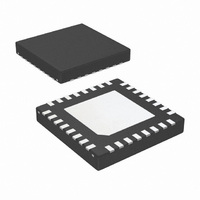
ADC14C080CISQ/NOPB National Semiconductor, ADC14C080CISQ/NOPB Datasheet - Page 6

ADC14C080CISQ/NOPB
Manufacturer Part Number
ADC14C080CISQ/NOPB
Description
ADC 14BIT 65/80MSPS 32-LLP
Manufacturer
National Semiconductor
Series
PowerWise®r
Datasheet
1.ADC14C080CISQENOPB.pdf
(24 pages)
Specifications of ADC14C080CISQ/NOPB
Number Of Bits
14
Sampling Rate (per Second)
80M
Data Interface
Parallel
Number Of Converters
1
Power Dissipation (max)
300mW
Voltage Supply Source
Single Supply
Operating Temperature
-40°C ~ 85°C
Mounting Type
Surface Mount
Package / Case
32-WFQFN Exposed Pad
Lead Free Status / RoHS Status
Lead free / RoHS Compliant
Other names
ADC14C080CISQ
Available stocks
Company
Part Number
Manufacturer
Quantity
Price
Company:
Part Number:
ADC14C080CISQ/NOPB
Manufacturer:
NS
Quantity:
6 218
www.national.com
V
Ext V
DYNAMIC CONVERTER CHARACTERISTICS, A
FPBW
SNR
SFDR
ENOB
THD
H2
H3
SINAD
IMD
DIGITAL INPUT CHARACTERISTICS (CLK, PD)
V
V
I
I
C
Symbol
Symbol
Symbol
IN(1)
IN(0)
RN
IN(1)
IN(0)
IN
ADC14C080 Dynamic Converter Electrical Characteristics
Unless otherwise specified, the following specifications apply: AGND = DRGND = 0V, V
+1.2V, f
limits apply for T
ADC14C080 Logic and Power Supply Electrical Characteristics
Unless otherwise specified, the following specifications apply: AGND = DRGND = 0V, V
+1.2V, f
limits apply for T
REF
CLK
CLK
Logical “1” Input Voltage
Logical “0” Input Voltage
Logical “1” Input Current
Logical “0” Input Current
Digital Input Capacitance
Full Power Bandwidth
Signal-to-Noise Ratio
Spurious Free Dynamic Range
Effective Number of Bits
Total Harmonic Disortion
Second Harmonic Distortion
Third Harmonic Distortion
Signal-to-Noise and Distortion Ratio
Intermodulation Distortion
Internal Reference bottom
External Reference Voltage
= 80 MHz, 50% Duty Cycle, DCS Disabled, V
= 80 MHz, 50% Duty Cycle, DCS Disabled, V
MIN
MIN
≤
≤
Parameter
Parameter
Parameter
T
T
A
A
≤
≤
T
T
MAX
MAX
. All other limits apply for T
. All other limits apply for T
IN
(Note 13)
(Note 13)
V
V
V
V
-1 dBFS Input, −3 dB Corner
f
D
D
IN
IN
= -1dBFS
IN
= 3.6V
= 3.0V
= 19.5MHz and 20.5MHz, each -7dBFS
= 3.3V
= 0V
CM
CM
= V
= V
A
A
= 25°C (Notes 8, 9)
= 25°C (Notes 8, 9)
CMO
f
f
f
f
f
f
f
CMO
6
Conditions
f
f
IN
f
f
IN
f
f
IN
f
f
IN
f
f
IN
f
f
IN
f
f
IN
Conditions
Conditions
IN
IN
IN
IN
IN
IN
IN
IN
IN
IN
IN
IN
IN
IN
= 170 MHz
= 170 MHz
= 170 MHz
= 170 MHz
= 170 MHz
= 170 MHz
= 170 MHz
= 10 MHz
= 70 MHz
= 10 MHz
= 70 MHz
= 10 MHz
= 70 MHz
= 10 MHz
= 70 MHz
= 10 MHz
= 70 MHz
= 10 MHz
= 70 MHz
= 10 MHz
= 70 MHz
, C
, C
L
L
= 5 pF/pin, . Typical values are for T
= 5 pF/pin. Typical values are for T
A
A
= +3.0V, V
= +3.0V, V
(Note 10)
(Note 10)
Typical
Typical
(Note 10)
0.98
1.20
−100
Typical
74.2
70.5
11.6
11.4
71.8
70.2
−90
−85
−85
−95
−86
−90
−88
−88
1.0
-82
72
90
88
86
12
74
−10
10
5
DR
DR
= +2.5V, Internal V
= +2.5V, Internal V
Limits
Limits
1.176
1.224
0.89
1.06
-80.5
11.1
68.6
-82
-82
69
82
Limits
A
A
= 25°C. Boldface
2.0
0.8
= 25°C. Boldface
(Limits)
V (max)
V (max)
(Limits)
(Note 2)
V (min)
V (min)
Units
Units
dBFS
dBFS
dBFS
dBFS
dBFS
dBFS
dBFS
dBFS
dBFS
dBFS
dBFS
dBFS
dBFS
dBFS
dBFS
dBFS
dBFS
dBFS
dBFS
GHz
(Limits)
V (max)
Bits
Bits
Bits
V (min)
Units
REF
REF
µA
µA
pF
=
=


