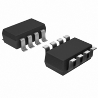
AD7453BRT-R2 Analog Devices Inc, AD7453BRT-R2 Datasheet - Page 5

AD7453BRT-R2
Manufacturer Part Number
AD7453BRT-R2
Description
IC ADC 12BIT 555KSPS SOT23-8
Manufacturer
Analog Devices Inc
Datasheet
1.AD7453BRTZ-R2.pdf
(20 pages)
Specifications of AD7453BRT-R2
Rohs Status
RoHS non-compliant
Design Resources
Measuring -48 V High-Side Current Using AD629, AD8603, AD780, and AD7453 (CN0100)
Number Of Bits
12
Sampling Rate (per Second)
555k
Data Interface
DSP, MICROWIRE™, QSPI™, Serial, SPI™
Number Of Converters
1
Power Dissipation (max)
7.25mW
Voltage Supply Source
Single Supply
Operating Temperature
-40°C ~ 85°C
Mounting Type
Surface Mount
Package / Case
SOT-23-8
Other names
AD7453BRT-R2TR
TIMING SPECIFICATIONS
Guaranteed by characterization. All input signals are specified with tr = tf = 5 ns (10% to 90% of V
level of 1.6 V.
See Figure 2 and the Serial Interface section.
V
Table 2.
Parameter
f
t
t
t
t
t
t
t
t
t
t
t
1
2
3
4
SCLK
CONVERT
QUIET
1
2
3
4
5
6
7
8
POWER-UP
Mark/space ratio for the SCLK input is 40/60 to 60/40.
Measured with the load circuit of
cross 0.4 V or 2.0 V for V
t
back to remove the effects of charging or discharging the 25 pF capacitor. This means that the time, t
time of the part and is independent of the bus loading.
See Power-Up Time section.
2
2
3
8
DD
is derived from the measured time taken by the data outputs to change 0.5 V when loaded with the circuit of
1
= 2.7 V to 5.25 V, f
4
Limit at T
10
10
16 × t
1.6
60
10
10
20
40
0.4 t
0.4 t
10
10
35
1
SDATA
SCLK
CS
SCLK
SCLK
SCLK
DD
= 3 V.
SCLK
t
t
2
3
MIN
= 10 MHz, f
, T
Figure 3
0
MAX
1
4 LEADING ZEROS
0
and defined as the time required for the output to cross 0.8 V or 2.4 V with V
Unit
kHz min
MHz max
µs max
ns min
ns min
ns min
ns max
ns max
ns min
ns min
ns min
ns min
ns max
µs max
S
2
= 555 kSPS, V
0
3
t
Figure 2. AD7453 Serial Interface Timing Diagram
Description
t
Minimum quiet time between the end of a serial read and the next falling edge of CS
Minimum CS pulse width
CS falling edge to SCLK falling edge setup time
Delay from CS falling edge until SDATA three-state disabled
Data access time after SCLK falling edge
SCLK high pulse width
SCLK low pulse width
SCLK edge to data valid hold time
SCLK falling edge to SDATA three-state enabled
SCLK falling edge to SDATA three-state enabled
Power-up time from full power-down
4
SCLK
0
= 1/f
REF
4
DB11
= 2.5 V, T
t
SCLK
5
Rev. B | Page 5 of 20
5
t
DB10
t
7
CONVERT
A
= T
MIN
to T
13
B
MAX
DB2
, unless otherwise noted.
8
14
t
, quoted in the timing characteristics is the true bus relinquish
6
DB1
15
Figure 3.
t
DB0
8
DD
DD
= 5 V, and the time required for an output to
The measured number is then extrapolated
) and timed from a voltage
16
THREE-STATE
t
QUIET
t
1
AD7453


