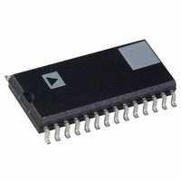
AD1877JR Analog Devices Inc, AD1877JR Datasheet - Page 11

AD1877JR
Manufacturer Part Number
AD1877JR
Description
IC ADC STEREO 16BIT 28-SOIC
Manufacturer
Analog Devices Inc
Datasheet
1.AD1877JRZ.pdf
(20 pages)
Specifications of AD1877JR
Rohs Status
RoHS non-compliant
Number Of Bits
16
Sampling Rate (per Second)
48k
Data Interface
Serial
Number Of Converters
2
Power Dissipation (max)
315mW
Voltage Supply Source
Analog and Digital
Operating Temperature
0°C ~ 70°C
Mounting Type
Surface Mount
Package / Case
28-SOIC (0.300", 7.50mm Width)
Available stocks
Company
Part Number
Manufacturer
Quantity
Price
Part Number:
AD1877JR
Manufacturer:
ADI/亚德诺
Quantity:
20 000
Part Number:
AD1877JRZ
Manufacturer:
ADI/亚德诺
Quantity:
20 000
REV. A
Two modes deserve special discussion. The first special mode,
“Slave Mode, Data Position Controlled by WCLK Input” (S/M
= HI, RLJUST = HI, MSBDLY = LO), shown in Figure 8, is
the only mode in which WCLK is an input. The 16-bit output
data words can be placed at user-defined locations within 32-bit
fields. The MSB will appear in the BCLK period after WCLK is
detected HI by the BCLK sampling edge. If WCLK is HI dur-
ing the first BCLK of the 32-bit field (if WCLK is tied HI for
example), then the MSB of the output word will be valid on the
sampling edge of the second BCLK. The effect is to delay the
MSB for one bit clock cycle into the field, making the output
data compatible at the data format level with the I
mat. Note that the relative placement of the WCLK input can
vary from 32-bit field to 32-bit field, even within the same
64-bit frame. For example, within a single 64-bit frame, the left
word could be right justified (by pulsing WCLK HI on the 16th
BCLK) and the right word could be in an I
format (by having WCLK HI at the beginning of the second field).
In the second special mode “Master Mode, Right-Justified with
MSB Delay, WCLK Pulsed in 17th Cycle” (S/M = LO,
RLJUST = HI, MSBDLY = LO), shown in Figure 12, WCLK
is an output and is pulsed for one cycle by the AD1877. The
MSB is valid on the 18th BCLK sampling edge, and the LSB
extends into the first BCLK period of the next 32-bit field.
Timing Parameters
For master modes, a BCLK transmitting edge (labeled “XMIT”)
will be delayed from a CLKIN rising edge by t
in Figure 17. A LRCK transition will be delayed from a BCLK
transmitting edge by t
delayed from a BCLK transmitting edge by t
falling edge will be delayed from a BCLK transmitting edge by
t
transmitting edge of BCLK by t
For slave modes, an LRCK transition must be setup to a BCLK
sampling edge (labeled “SAMPLE”) by t
and TAG outputs will be delayed from an LRCK transition by
t
BCLK transmitting edge by t
Position Controlled by WCLK Input,” WCLK must be setup to
a BCLK sampling edge by t
DLYBWF
DLYLRDT
. The DATA and TAG outputs will be delayed from a
, and DATA and TAG outputs will be delayed from
DLYBLR
SETWBS
. A WCLK rising edge will be
DLYBDT
DLYDT
.
. For “Slave Mode, Data
.
SETLRBS.
2
DLYBWR
S-compatible data
DLYCKB
The DATA
, and a WCLK
2
S data for-
, as shown
–11–
For both master and slave modes, BCLK must have a minimum
LO pulsewidth of t
The AD1877 CLKIN and RESET timing is shown in Figure
19. CLKIN must have a minimum LO pulsewidth of t
a minimum HI pulse width of t
CLKIN is given by t
pulsewidth of t
requirements for RESET.
Synchronizing Multiple AD1877s
Multiple AD1877s can be synchronized by making all the
AD1877s serial port slaves. This option is illustrated in
Figure 6. See the “Reset, Autocalibration and Power Down”
section above for additional information.
Figure 6. Synchronizing Multiple AD1877s
RPWL
BPWL
. Note that there are no setup or hold time
CLKIN
RESET
CLKIN
RESET
CLKIN
RESET
CLKIN
#1 AD1877
SLAVE MODE
#2 AD1877
SLAVE MODE
#N AD1877
SLAVE MODE
, and a minimum HI pulsewidth of t
. RESET must have a minimum LO
CPWH
. The minimum period of
WCLK
WCLK
WCLK
DATA
BCLK
LRCK
DATA
BCLK
LRCK
DATA
BCLK
LRCK
SOURCE
CLOCK
AD1877
CPWL
BPWH
, and
.


