AD7485BST Analog Devices Inc, AD7485BST Datasheet
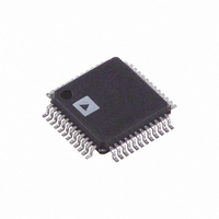
IC ADC 14BIT SAR 1MSPS 48-LQFP

AD7485BST

Manufacturer Part Number
AD7485BST
Description
IC ADC 14BIT SAR 1MSPS 48-LQFP
Manufacturer
Analog Devices Inc
Datasheet

Specifications of AD7485BST

Rohs Status
RoHS non-compliant
Number Of Bits
14
Sampling Rate (per Second)
1M
Data Interface
Serial
Number Of Converters
1
Power Dissipation (max)
80mW
Voltage Supply Source
Analog and Digital
Operating Temperature
-40°C ~ 85°C
Mounting Type
Surface Mount
Package / Case
48-LQFP

Available stocks

Company
Part Number
Manufacturer
Quantity
Price
Part Number:
AD7485BST
Manufacturer:
ADI
Quantity:
238
Part Number:
AD7485BSTZ
Manufacturer:
ADI
Quantity:
240
Part Number:
AD7485BSTZ
Manufacturer:
Analog Devices Inc
Quantity:
10 000
Part Number:
AD7485BSTZ
Manufacturer:
ADI/亚德诺
Quantity:
20 000
a
GENERAL DESCRIPTION
The AD7485 is a 14-bit, high speed, low power, successive-
approximation ADC. The part features a serial interface with
throughput rates up to 1 MSPS. The part contains a low noise,
wide bandwidth track-and-hold that can handle input frequencies
in excess of 40 MHz.
The conversion process is a proprietary algorithmic successive-
approximation technique. The input signal is sampled and a
conversion is initiated on the falling edge of the CONVST signal.
The conversion process is controlled by an external master
clock. Interfacing is via standard serial signal lines, making the
part directly compatible with microcontrollers and DSPs.
The AD7485 provides excellent ac and dc performance specifi-
cations. Factory trimming ensures high dc accuracy resulting in
very low INL, DNL, offset, and gain errors.
The part uses advanced design techniques to achieve very low
power dissipation at high throughput rates. Power consumption
in the normal mode of operation is 80 mW. There are two power-
saving modes: a NAP mode keeps reference circuitry alive for
quick power-up and consumes 3 mW, while a STANDBY mode
reduces power consumption to a mere 10 µW.
REV.
Information furnished by Analog Devices is believed to be accurate and
reliable. However, no responsibility is assumed by Analog Devices for its
use, nor for any infringements of patents or other rights of third parties that
may result from its use. No license is granted by implication or otherwise
under any patent or patent rights of Analog Devices.
FEATURES
Fast Throughput Rate: 1 MSPS
Wide Input Bandwidth: 40 MHz
Excellent DC Accuracy Performance
Flexible Serial Interface
Low Power:
STANDBY Mode: 2 A Max
Single 5 V Supply Operation
Internal 2.5 V Reference
Full-Scale Overrange Indication
80 mW (Full Power) and 3 mW (NAP Mode)
A
The AD7485 features an on-board 2.5 V reference, but the part can
also accommodate an externally provided 2.5 V reference source.
The nominal analog input range is 0 V to 2.5 V.
The AD7485 also provides the user with overrange indication via a
fifteenth bit. If the analog input range strays outside the 0 V to
2.5 V input range, the fifteenth data bit is set to a logic high.
The AD7485 is powered from a 4.75 V to 5.25 V supply. The
part also provides a V
voltage levels for the digital interface lines. The range for this
V
48-lead LQFP package and is specified over a –40°C to +85°C
temperature range.
One Technology Way, P.O. Box 9106, Norwood, MA 02062-9106, U.S.A.
Tel: 781/329-4700
Fax:
DRIVE
1 MSPS, Serial 14-Bit SAR ADC
781/461-3113
REFSEL
CONVST
pin is from 2.7 V to 5.25 V. The part is housed in a
RESET
STBY
NAP
VIN
FUNCTIONAL BLOCK DIAGRAM
AV
DD
REFERENCE
T/H
AGND
2.5 V
AD7485
DRIVE
LOGIC AND I/O
REGISTERS
C
pin that allows the user to set the
CONTROL
BIAS
ALGORITHMIC
DV
14-BIT
DD
BUF
SAR
© Analog Devices, Inc.,
V
DRIVE
AD7485
DGND
www.analog.com
REFOUT
REFIN
SDO
MCLK
TFS
SCO
SMODE
2010

Related parts for AD7485BST

AD7485BST Summary of contents

Page 1

FEATURES Fast Throughput Rate: 1 MSPS Wide Input Bandwidth: 40 MHz Excellent DC Accuracy Performance Flexible Serial Interface Low Power (Full Power) and 3 mW (NAP Mode) STANDBY Mode Max Single 5 V Supply Operation ...

Page 2

AD7485–SPECIFICATIONS Parameter 2, 3 DYNAMIC PERFORMANCE Signal to Noise + Distortion (SINAD) 4 Total Harmonic Distortion (THD) Peak Harmonic or Spurious Noise (SFDR) 4 Intermodulation Distortion (IMD) Second-Order Terms Third-Order Terms Aperture Delay Full Power Bandwidth DC ACCURACY Resolution 4 ...

Page 3

Parameter POWER REQUIREMENTS DRIVE I DD Normal Mode (Static) Normal Mode (Operational) NAP Mode 8 STANDBY Mode Power Dissipation Normal Mode (Operational) NAP Mode 8 STANDBY Mode NOTES 1 Temperature ranges as follows: –40°C to +85°C. 2 ...

Page 4

AD7485 ABSOLUTE MAXIMUM RATINGS 25°C, unless otherwise noted GND . . . . . . . . . . . . . . . . . . . . . . . . . . ...

Page 5

Pin No. Mnemonic Description Positive Power Supply for Analog Circuitry Decoupling Pin for Internal Bias Voltage capacitor should be placed between this pin BIAS and AGND ...

Page 6

AD7485 TERMINOLOGY Integral Nonlinearity This is the maximum deviation from a straight line passing through the endpoints of the ADC transfer function. The end- points of the transfer function are zero scale, a point 1/2 LSB below the first code ...

Page 7

ADC CODE TPC 1. Typical DNL 1.0 0.8 0.6 0.4 0.2 0 –0.2 –0.4 –0.6 –0.8 –1.0 0 4096 8192 ADC CODE TPC 2. Typical INL ...

Page 8

AD7485 0 –20 –40 –60 –80 –100 –120 –140 0 100 200 300 FREQUENCY – kHz TPC 7. 64k FFT Plot with 10 kHz Input Tone + 100 SIGNAL 1k AD829 BIAS VOLTAGE ...

Page 9

CIRCUIT DESCRIPTION CONVERTER OPERATION The AD7485 is a 14-bit algorithmic successive-approximation analog-to-digital converter based around a capacitive DAC. It pro- vides the user with track-and-hold, reference, an A/D converter, and versatile interface logic functions on a single chip. The analog ...

Page 10

AD7485 Figure 7 shows the AD7485 conversion sequence operating in normal mode CONVST TFS READ DATA 960ns Figure 7. Normal Mode Power Dissipation In NAP mode, all the internal circuitry except for the internal reference is powered down. ...

Page 11

SERIAL INTERFACE The AD7485 has two serial interface modes, selected by the state of the SMODE pin. In both these modes, the MCLK pin must be supplied with a clock signal of between 10 kHz and 25 MHz. This MCLK ...

Page 12

AD7485 Board Layout and Grounding To obtain optimum performance from the AD7485 recom- mended that a printed circuit board with a minimum of three layers is used. One of these layers, preferably the middle layer, should be as ...

Page 13

CONVST t 7 MCLK SCO t 8 SDO D14 D13 D12 D11 t 12 CONVST t 7 MCLK t 14 SCO SDO D14 D13 D12 D11 t 15 TFS MCLK t 19 SCO REV ...

Page 14

... PLANE VIEW A ROTATED 90° CCW ORDERING GUIDE 1 Model Temperature Range AD7485BSTZ −40°C to +85° RoHS Compliant Part. REVISION HISTORY 4/10—Rev Rev. A Changes to Specifications Table ............................................................. 3 ©2002-2010 Analog Devices, Inc. All rights reserved. Trademarks and registered trademarks are the property of their respective owners. ...

Related keywords