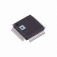
AD7482BST Analog Devices Inc, AD7482BST Datasheet

AD7482BST
Specifications of AD7482BST
Available stocks
Related parts for AD7482BST
AD7482BST Summary of contents
Page 1
FEATURES Fast throughput rate: 3 MSPS Wide input bandwidth: 40 MHz No pipeline delays with SAR ADC Excellent dc accuracy performance 2 parallel interface modes Low power (full power) and 2.5 mW (nap mode) Standby mode: 2 µA ...
Page 2
AD7482 TABLE OF CONTENTS Features .............................................................................................. 1 Functional Block Diagram .............................................................. 1 General Description ......................................................................... 1 Revision History ............................................................................... 2 Specifications ..................................................................................... 3 Timing Characteristics ................................................................ 5 Absolute Maximum Ratings ............................................................ 6 ESD Caution .................................................................................. 6 Pin Configuration and Function ...
Page 3
SPECIFICATIONS AV / ± 5%, AGND = DGND = 5.25 V, unless otherwise noted. The operating temperature range is −40°C to +85°C. Table 1. Parameter DYNAMIC PERFORMANCE 1, 2 Signal-to-Noise + ...
Page 4
AD7482 Parameter LOGIC INPUTS Input High Voltage, V INH Input Low Voltage, V INL Input Current Input Capacitance LOGIC OUTPUTS Output High Voltage Output Low Voltage Floating State Leakage Current Floating ...
Page 5
TIMING CHARACTERISTICS AV / ± 5%, AGND = DGND = unless otherwise noted. Table 2. Parameter 1 DATA READ Conversion Time Quiet Time Before Conversion Start Pulse width CONVST CONVST Falling Edge ...
Page 6
AD7482 ABSOLUTE MAXIMUM RATINGS T = 25°C, unless otherwise noted. A Table 3. Parameter AV to AGND DGND DGND DRIVE Analog Input Voltage to AGND Digital Input Voltage to DGND REFIN to AGND Input ...
Page 7
PIN CONFIGURATION AND FUNCTION DESCRIPTIONS Table 4. Pin Function Descriptions Pin No. Mnemonic Description Positive Power Supply for Analog Circuitry Decoupling Pin for Internal Bias Voltage capacitor should be ...
Page 8
AD7482 Pin No. Mnemonic Description 30, 31 DGND Ground Reference for Digital Circuitry Logic Power Supply Input. The voltage supplied at this pin determines at what voltage the interface logic of DRIVE the device operates. 40 D12 Data ...
Page 9
TYPICAL PERFORMANCE CHARACTERISTICS 0 –20 –40 –60 –80 –100 –120 0 200 400 600 800 FREQUENCY (kHz) Figure 3. 64k FFT Plot With 10 kHz Input Tone 1.013MHz IN SNR = 72.58dB SNR + D = 72.57dB ...
Page 10
AD7482 0 100mV p-p SINE WAVE ON SUPPLY PINS –10 –20 –30 –40 –50 –60 –70 –80 10 100 FREQUENCY (kHz) Figure 9. PSRR Without Decoupling 0.0004 0 –0.0004 –0.0008 –0.0012 –0.0016 –0.0020 1000 –55 –25 Figure 10. Reference Out ...
Page 11
TERMINOLOGY Integral Nonlinearity The integral nonlinearity is the maximum deviation from a straight line passing through the endpoints of the ADC transfer function. The endpoints of the transfer function are zero scale, a point 1/2 LSB below the first code ...
Page 12
AD7482 CIRCUIT DESCRIPTION CONVERTER OPERATION The AD7482 is a 12-bit algorithmic successive approximation ADC based around a capacitive DAC. It provides the user with track-and-hold, reference, an ADC, and versatile interface logic functions on a single chip. The normal analog ...
Page 13
For higher input bandwidth applications, the (also available as a dual AD8022 op amp) is the recommended choice to drive the AD7482. Figure 15 shows the analog input circuit used to obtain the data for the FFT plot shown in ...
Page 14
AD7482 Figure 18 shows the AD7482 conversion sequence when the part is put into nap mode after each conversion. 600ns 1400ns NAP 300ns CONVST BUSY 2µs Figure 18. Nap Mode Power Dissipation Figure 19 and Figure 20 show a typical ...
Page 15
V /4096 REF 111...000 011...111 000...010 000...001 000...000 0.5LSB 0V –OFFSET ANALOG INPUT Figure 22. Transfer Characteristic with Negative Offset Table 5 shows the expected ADC result for a given analog input voltage with different offset ...
Page 16
AD7482 Data must not be read from the AD7482 while a conversion is taking place. For this reason, if operating the AD7482 at through- put speeds greater than 2.5 MSPS necessary to tie both the CS pin and ...
Page 17
BOARD LAYOUT AND GROUNDING For optimum performance from the AD7482 recommended that a PCB with a minimum of three layers be used. One of these layers, preferably the middle layer, should be as complete a ground plane as ...
Page 18
AD7482 CONVST BUSY WRITE RD D[12:0] CONVST CS RD WRITE D[12:0] CONVST BUSY D[12:0] CONVST BUSY D[12:0] t CONV DATA VALID Figure 29. Parallel Mode Read Cycle t ...
Page 19
... VIEW A ROTATED 90° CCW ORDERING GUIDE Model 1 Temperature Range AD7482ASTZ −40°C to +85°C AD7482BSTZ −40°C to +85°C EVAL-AD7482CB EVAL-CONTROLBRD2Z RoHS Compliant Part. 2 This can be used either as a standalone evaluation board or in conjunction with the controller board for evaluation/demonstration purposes. ...
Page 20
AD7482 NOTES ©2002–2009 Analog Devices, Inc. All rights reserved. Trademarks and registered trademarks are the property of their respective owners. D02638-0-12/09(B) Rev Page ...


