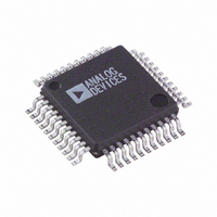
AD7865BS-1 Analog Devices Inc, AD7865BS-1 Datasheet - Page 10

AD7865BS-1
Manufacturer Part Number
AD7865BS-1
Description
IC ADC 14BIT 4CH 5V 44-MQFP
Manufacturer
Analog Devices Inc
Specifications of AD7865BS-1
Rohs Status
RoHS non-compliant
Number Of Bits
14
Sampling Rate (per Second)
350k
Data Interface
Parallel
Number Of Converters
1
Power Dissipation (max)
160mW
Voltage Supply Source
Analog and Digital
Operating Temperature
-40°C ~ 85°C
Mounting Type
Surface Mount
Package / Case
44-MQFP, 44-PQFP
Available stocks
Company
Part Number
Manufacturer
Quantity
Price
Company:
Part Number:
AD7865BS-1
Manufacturer:
ADI
Quantity:
329
AD7865
AD7865-1
Figure 2 shows the analog input section of the AD7865-1. Each
input can be configured for 5 V or 10 V operation on the
AD7865-1. For 5 V operation, the V
tied together and the input voltage is applied to both. For 10 V
operation, the V
age is applied to the V
symmetrical and fully interchangeable. Thus for ease of PCB
layout on the 10 V range, the input voltage may be applied to
the V
For the AD7865-1, R1 = 4 k , R2 = 16 k
R4 = 8 k . The resistor input stage is followed by the high
input impedance stage of the track/hold amplifier.
The designed code transitions take place midway between suc-
cessive integer LSB values (i.e., 1/2 LSB, 3/2 LSBs, 5/2 LSBs
etc.) LSB size is given by the formula, 1 LSB = FSR/16384. For
the 5 V range, 1 LSB = 10 V/16384 = 610.4 V. For the 10 V
range, 1 LSB = 20 V/16384 = 1.22 mV. Output coding is twos
complement binary with 1 LSB = FSR/16384. The ideal input/
output transfer function for the AD7865-1 is shown in Table I.
Analog Input
+FSR/2 – 3/2 LSB
+FSR/2 – 5/2 LSB
+FSR/2 – 7/2 LSB
AGND + 3/2 LSB
AGND + 1/2 LSB
AGND – 1/2 LSB
AGND – 3/2 LSB
–FSR/2 + 5/2 LSB
–FSR/2 + 3/2 LSB
–FSR/2 + 1/2 LSB
NOTES
1
2
FSR is full-scale range and is 20 V for the 10 V range and 10 V for the 5 V
1 LSB = FSR/16384 = 1.22 mV ( 10 V—AD7865-1) and 610.4 mV ( 5 V—
range, with V
AD7865-1) with V
Table I. Ideal Input/Output Code Table for the AD7865-1
INxB
V
V
V
INxB
INxA
REF
Figure 2. AD7865-1 Analog Input Structure
input while the V
REF
6k
1
= +2.5 V.
REF
INxB
2
= +2.5 V.
R2
R3
input is tied to AGND and the input volt-
INxA
REFERENCE
input. The V
INxA
R1
R4
+2.5V
GND
Digital Output Code Transition
011 . . . 110 to 011 . . . 111
011 . . . 101 to 011 . . . 110
011 . . . 100 to 011 . . . 101
000 . . . 001 to 000 . . . 010
000 . . . 000 to 000 . . . 001
111 . . . 111 to 000 . . . 000
111 . . . 110 to 111 . . . 111
100 . . . 010 to 100 . . . 011
100 . . . 001 to 100 . . . 010
100 . . . 000 to 100 . . . 001
input is tied to AGND.
TO ADC
REFERENCE
CIRCUITRY
TRACK/
HOLD
INxA
INxA
and V
AD7865-1
and V
TO INTERNAL
COMPARATOR
R3 = 16 k and
INxB
INxB
inputs are
inputs are
–10–
AD7865-2
Figure 3 shows the analog input section of the AD7865-2. Each
input can be configured for 0 V to +5 V operation or 0 V to +2.5 V
operation. For the 0 V to +5 V operation, the V
to AGND and the input voltage is applied to V
0 V to +2.5 V operation, the V
together and the input voltage is applied to both. The V
V
ease of PCB layout on the 0 V to +5 V range the input voltage
may be applied to the V
AGND.
For the AD7865-2, R1 = 4 k and R2 = 4 k . Once again, the
designed code transitions occur on successive integer LSB val-
ues. Output coding is straight (natural) binary with 1 LSB =
FSR/16384 = +2.5 V/16384 = 0.153 mV, and +5 V/16384 =
0.305 mV, for 0 V to +2.5 V and 0 V to +5 V options respec-
tively. Table II shows the ideal input and output transfer
function for the AD7865-2.
Analog Input
+FSR/2 – 3/2 LSB
+FSR/2 – 5/2 LSB
+FSR/2 – 7/2 LSB
AGND + 5/2 LSB
AGND + 3/2 LSB
AGND – 1/2 LSB
NOTES
1
2
FSR is full-scale range and is 0 V to +2.5 V and 0 V to +5 V for AD7865-2
1 LSB = FSR/16384 and is 0.153 mV (0 V to +2.5 V) and 0.305 mV (0 V to +5 V)
with V
for AD7865-2) with V
INxB
Table II. Ideal Input/Output Code Table for the AD7865-2
V
inputs are symmetrical and fully interchangeable. Thus for
V
REF
V
INxA
INxB
REF
Figure 3. AD7865-2 Analog Input Structure
= +2.5 V.
6k
1
REF
2
R1
R2
= +2.5 V.
INxB
REFERENCE
input while the V
Digital Output Code Transition
111 . . . 110 to 111 . . . 111
111 . . . 101 to 111 . . . 110
111 . . . 100 to 111 . . . 101
000 . . . 010 to 000 . . . 011
000 . . . 001 to 000 . . . 010
000 . . . 000 to 000 . . . 001
+2.5V
INxA
and V
TO ADC
REFERENCE
CIRCUITRY
TRACK/
HOLD
INxB
AD7865-2
TO INTERNAL
COMPARATOR
inputs are tied
INxA
INxA
INxB
input is tied to
input. For
input is tied
INxA
REV. A
and


