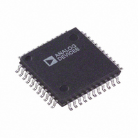
AD9054ABST-135 Analog Devices Inc, AD9054ABST-135 Datasheet - Page 13

AD9054ABST-135
Manufacturer Part Number
AD9054ABST-135
Description
IC ADC 8BIT 135MSPS 44-LQFP
Manufacturer
Analog Devices Inc
Datasheet
1.AD9054ABSTZ-135.pdf
(20 pages)
Specifications of AD9054ABST-135
Rohs Status
RoHS non-compliant
Number Of Bits
8
Sampling Rate (per Second)
135M
Data Interface
Parallel
Number Of Converters
1
Power Dissipation (max)
700mW
Voltage Supply Source
Single Supply
Operating Temperature
-40°C ~ 85°C
Mounting Type
Surface Mount
Package / Case
44-LQFP
Available stocks
Company
Part Number
Manufacturer
Quantity
Price
Company:
Part Number:
AD9054ABST-135
Manufacturer:
FUJI
Quantity:
149
Company:
Part Number:
AD9054ABST-135
Manufacturer:
ADI
Quantity:
225
Part Number:
AD9054ABST-135
Manufacturer:
ADI/亚德诺
Quantity:
20 000
Digital Inputs
SNR performance is directly related to the sampling clock sta-
bility in A/D converters, particularly for high input frequencies
and wide bandwidths. A low jitter clock (<10 ps @ 100 MHz) is
essential for optimum performance when digitizing signals that
are not presampled.
ENCODE and Data Select (DS) can be driven differentially or
single-ended. For single-ended operation, the complement
inputs (ENCODE, DS) are internally biased to V
by a high impedance on-chip resistor divider (Figure 5), but
they may be externally driven to establish an alternate threshold
if desired. A 0.1 µF decoupling capacitor to ground is sufficient
to maintain a threshold appropriate for TTL or CMOS logic.
When driven differentially, ENCODE and DS will accommo-
date differential signals centered between 1.5 V and 4.5 V with
a total differential swing ≥800 mV (V
Note the 6-diode clock input protection circuitry in Figure 5.
This limits the differential input voltage to ~ ± 2.1 V. When the
diodes turn on, current is limited by the 300 Ω series resistor.
Exceeding 2.1 V across the differential inputs will have no
impact on the performance of the converter, but be aware of the
clock signal distortion that may be produced by the nonlinear
impedance at the converter.
Single Port Mode
When operated in a Single Port mode (DEMUX = HIGH), the
timing of the AD9054A is similar to any high speed A/D Con-
verter (Figure 1).
A sample is taken on every rising edge of ENCODE, and the
resulting data is produced on the output pins following the
FOURTH rising edge of ENCODE after the sample was taken
(four pipeline delays). The output data are valid t
rising edge of ENCODE, and remain valid until at least t
the next rising edge of ENCODE.
The maximum clock rate is specified as 100 MSPS. This is
recommended because the guaranteed output data valid time
equals the Clock Period (1/f
Delay (t
4.8 ns at 100 MHz. This is about as fast as standard logic is able
to capture the data with reasonable design margins. The AD9054A
will operate faster in single-channel mode if you are able to
capture the data.
CLOCK
CLOCK
CLOCK
0.1 F
PD
b. Driving Differential Inputs Single-Endedly
a. Driving Differential Inputs Differentially
) plus the Output Valid Time (t
ENC
ENC
ENC
ENC
V
V
V
V
V
V
IC M
IC M
IH D
IH D
IL D
IL D
S
) minus the Output Propagation
ID
≥ 400 mV).
V
V
V
ID
ID
), which comes to
DD
PD
/3 (~1.5 V)
after the
V
after
When operating in Single-Channel Mode, the outputs at Port B
are held static in a random state.
Figure 10 shows the AD9054A used in single-channel output
mode. The analog input (±0.5 V) is ac coupled and the ENCODE
input is driven by a TTL level signal. The chip’s internal refer-
ence is used.
Dual Port Mode
In Dual Port Mode (DEMUX = LOW), the conversion results
are alternated between the two output ports (Figure 2). This
limits the data output rate at either port to 1/2 the conversion
rate (ENCODE), and supports conversion at up to 200 MSPS
with TTL/CMOS compatible interfaces. Dual Channel Mode is
required for guaranteed operation above 100 MSPS, but may be
enabled at any specified conversion rate.
The multiplexing is controlled internally via a clock divider,
which introduces a degree of ambiguity in the port assignments.
Figure 2 illustrates that, prior to synchronization, either Port A
or Port B may produce the even or odd samples. This is resolved
by exercising the Data Sync (DS) control, a differential input
(identical to the ENCODE input), which facilitates operation at
high speed.
At least once after power-up, and prior to using the conversion
data, the part needs to be synchronized by a falling edge (or a
positive-going pulse) on DS (observing setup and hold times
with respect to ENCODE). If the converter’s internal timing is
in conflict with the DS signal when it is exercised, then two data
samples (one on each port) are corrupted as the converter is
resynchronized. The converter then produces data with a
known phase relationship from that point forward.
Note that if the converter is already properly synchronized, the
DS pulse has no effect on the output data. This allows the con-
verter to be continuously resynchronized by a pulse at 1/2 the
ENCODE rate. This signal is often available within a system, as
it represents the master clock rate for the demultiplexed output
data. Of course, a single DS signal may be used to synchronize
multiple A/D converters in a multichannel system.
CLOCK
VIN
0.1 F
0.1 F
5V
1k
VREF OUT
VREF IN
AIN
AIN
DEMUX
DS
AD9054A
DS ENC
NC
NC = NO CONNECT
ENC
AD9054A
0.1 F
A PORT


