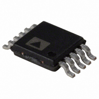
AD7992BRM-1 Analog Devices Inc, AD7992BRM-1 Datasheet - Page 26

AD7992BRM-1
Manufacturer Part Number
AD7992BRM-1
Description
IC ADC 12BIT 2CHAN I2C 10MSOP
Manufacturer
Analog Devices Inc
Datasheet
1.AD7992BRMZ-1.pdf
(28 pages)
Specifications of AD7992BRM-1
Number Of Bits
12
Sampling Rate (per Second)
79k
Data Interface
I²C, Serial
Number Of Converters
1
Power Dissipation (max)
2.2mW
Voltage Supply Source
Single Supply
Operating Temperature
-40°C ~ 125°C
Mounting Type
Surface Mount
Package / Case
10-TFSOP (0.118", 3.00mm Width)
For Use With
EVAL-AD7992CB - BOARD EVALUATION FOR AD7992
Lead Free Status / RoHS Status
Contains lead / RoHS non-compliant
AD7992
MODE 2 – COMMAND MODE
Mode 2 allows a conversion to be automatically initiated any
time a write operation occurs. In order to use this mode,
Command Bits C2 to C1 in the address pointer byte, shown in
Table 7, must be programmed. Command Bits C4 and C3 are
not used and should contain zeros at all times.
To select a channel for conversion in Mode 2, set the corres-
ponding channel command bit in the address pointer byte
(see Table 24). To select both analog input channels for con-
version, set both C1 and C2 to 1. When all four command
bits are 0, this mode is not used.
Figure 28 illustrates a 2-byte read operation from the conver-
sion result register. Prior to the read operation, ensure that the
address pointer is pointing to the conversion result register.
When the contents of the address pointer register are being
loaded, if Command Bits C2 or C1 are set, the AD7992 begins
to power up and convert upon the selected channel(s). Power-
up begins on the fifth SCL falling edge of the address point byte
(see point A in Figure 32). Table 24 shows the channel selection
in this mode via Command Bits C1 and C2 in the address
pointer register. The wake-up and conversion time together
should take approximately 3 µs, and the conversion begins
when the last Command Bit, C1, has been clocked in midway
through the write to the address pointer register. Following
this, the AD7992 must be addressed again to tell it that a read
operation is required. The read then takes place from the
conversion result register. This read accesses the result from
the conversion selected via the command bits. If Command Bits
C2, C1 are set to 1,1, a 4-byte read is necessary. The first read
SDA
SDA
SCL
SCL
Sr
S
1
1
7-BIT ADDRESS
7-BIT ADDRESS
ACK BY
AD7992
W
R
8
ACK BY
AD7992
A
A
9
9
Figure 32. Mode 2 Operation
1
1
Rev. 0 | Page 26 of 28
COMMAND/ADDRESS
FIRST DATA BYTE
POINT BYTE
(MSBs)
A
accesses the data from the conversion on V
takes place, a conversion occurs on V
accesses this data from V
operates.
After the conversion result has been read, and if further read
bytes are issued, the ADC continuously converts on the selected
input channel(s). This has the effect of increasing the overall
throughput rate of the ADC.
When operating the AD7992-1 in Mode 2 with high speed
mode, 3.4 MHz SCL, the conversion may not be complete
before the master tries to read the conversion result. In this
case, the AD7992-1 holds the SCL line low during the ACK
clock after the read address until the conversion is complete.
When the conversion is complete, the AD7992-1 releases the
SCL line and the master can then read the conversion result.
After a conversion is initiated in this mode by setting the
command bits in the address pointer byte, if the AD7992
receives a STOP or NACK from the master, the AD7992 stops
converting.
Table 24. Address Pointer Byte—Command Bits
C2
0
0
1
1
C1
0
1
0
1
Analog Input Channel
No conversion
Conversion on V
Conversion on V
Conversion on V
MASTER
ACK BY
ACK BY
AD7992
9
A
A
9
SECOND DATA BYTE
IN
(LSBs)
2. Figure 33 shows how this mode
IN
IN
IN
1
2
1 followed by conversion on V
IN
2. The second read
NACK BY
MASTER
A
IN
9
1. While this read
Sr/P
IN
2


