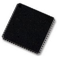
AD80192BCPZ-155 Analog Devices Inc, AD80192BCPZ-155 Datasheet - Page 11

AD80192BCPZ-155
Manufacturer Part Number
AD80192BCPZ-155
Description
IC ADC 14BIT 155MSPS 64LFCSP
Manufacturer
Analog Devices Inc
Datasheet
1.AD9640ABCPZ-80.pdf
(52 pages)
Specifications of AD80192BCPZ-155
Data Interface
Serial, SPI™
Number Of Bits
14
Sampling Rate (per Second)
155M
Number Of Converters
2
Voltage Supply Source
Analog and Digital
Operating Temperature
-40°C ~ 85°C
Mounting Type
Surface Mount
Package / Case
64-LFCSP
Resolution (bits)
14bit
Sampling Rate
150MSPS
Input Channel Type
Differential
Supply Voltage Range - Analog
1.7V To 1.9V
Digital Ic Case Style
CSP
No. Of Pins
64
Lead Free Status / RoHS Status
Lead free / RoHS Compliant
Parameter
OUT-OF-RANGE RECOVERY TIME
1
2
3
SWITCHING SPECIFICATIONS—AD9640ABCPZ-125, AD9640BCPZ-125, AD9640ABCPZ-150, AND
AD9640BCPZ-150
AVDD = 1.8 V, DVDD = 1.8V, DRVDD = 3.3 V, maximum sample rate, VIN = −1.0 dBFS differential input, 1.0 V internal reference, DCS
enabled, unless otherwise noted.
Table 7.
Parameter
CLOCK INPUT PARAMETERS
DATA OUTPUT PARAMETERS (DATA, FD)
OUT-OF-RANGE RECOVERY TIME
1
2
3
Conversion rate is the clock rate after the divider.
Output propagation delay is measured from CLK 50% transition to DATA 50% transition, with 5 pF load.
Wake-up time is dependent on the value of the decoupling capacitors.
Conversion rate is the clock rate after the divider.
Output propagation delay is measured from CLK 50% transition to DATA 50% transition, with 5 pF load.
Wake-up time is dependent on the value of the decoupling capacitors.
CMOS Mode Pipeline Delay (Latency)
Aperture Delay (t
Aperture Uncertainty (Jitter, t
Wake-Up Time
Input Clock Rate
Conversion Rate
CLK Period—Divide by 1 Mode (t
CLK Pulse Width High
CMOS Mode—DRVDD = 3.3 V
CMOS Mode—DRVDD = 1.8 V
LVDS Mode—DRVDD = 1.8 V
CMOS Mode Pipeline Delay (Latency)
LVDS Mode Pipeline Delay (Latency)
Channel A/Channel B
Aperture Delay (t
Aperture Uncertainty (Jitter, t
Wake-Up Time
LVDS Mode Pipeline Delay (Latency)
Data Propagation Delay (t
DCO Propagation Delay (t
Data Propagation Delay (t
DCO Propagation Delay (t
Setup Time (t
Hold Time (t
Data Propagation Delay (t
DCO Propagation Delay (t
Channel A/Channel B
DCS Enabled
DCS Disabled
Divide by 1 Mode, DCS Enabled
Divide by 1 Mode, DCS Disabled
Divide by 2 Mode, DCS Enabled
Divide by 3 Through 8, DCS Enabled
3
H
3
1
)
S
1
)
A
A
)
)
PD
DCO
PD
DCO
PD
DCO
J
J
)
)
)
)
)
2
2
2
)
)
)
CLK
)
Temperature
Full
Full
Full
Full
Full
Full
Full
Full
Full
Full
Full
Full
Full
Full
Full
Full
Full
Full
Full
Full
Full
Temp
Full
Full
Full
Full
Full
Min
Min
20
10
8
2.4
3.6
1.6
0.8
2.2
3.8
2.4
4.0
3.0
5.0
Rev. B | Page 11 of 52
AD9640ABCPZ-80
AD9640ABCPZ-125/
AD9640BCPZ-80
AD9640BCPZ-125
Typ
12
12/12.5
1.0
0.1
350
2
Typ
4
4
4.5
5.0
4.5
3.5
5.2
5.6
3.8
6.2
12
12/12.5
1.0
0.1
350
3
Max
Max
625
125
125
5.6
4.4
6.4
6.8
6.9
7.3
4.5
7.4
Min
Min
20
10
6.66
2.0
3.0
1.6
0.8
2.2
3.8
2.4
4.0
3.0
4.8
AD9640ABCPZ-105/
AD9640ABCPZ-150/
AD9640BCPZ-105
AD9640BCPZ-150
Typ
12
12/12.5
0.1
1.0
350
2
Typ
3.33
3.33
4.5
5.0
3.83
2.83
5.2
5.6
3.8
5.9
12
12/12.5
1.0
0.1
350
3
Max
Max
625
150
150
4.66
3.66
6.4
6.8
6.9
7.3
4.5
7.3
Unit
Cycles
Cycles
ns
ps rms
μs
Cycles
AD9640
Unit
MHz
MSPS
MSPS
ns
ns
ns
ns
ns
ns
ns
ns
ns
ns
ns
ns
ns
Cycles
Cycles
ns
ps rms
μs
Cycles


