604-00026 Parallax Inc, 604-00026 Datasheet - Page 12
604-00026
Manufacturer Part Number
604-00026
Description
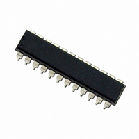
IC ADC 12BIT 8CH MAX1270 24-DIP
Manufacturer
Parallax Inc
Datasheet
1.604-00026.pdf
(20 pages)
Specifications of 604-00026
Number Of Bits
12
Sampling Rate (per Second)
110k
Data Interface
MICROWIRE™, QSPI™, Serial, SPI™
Number Of Converters
1
Power Dissipation (max)
1.07W
Voltage Supply Source
Single Supply
Operating Temperature
0°C ~ 70°C
Mounting Type
Through Hole
Package / Case
24-DIP
Lead Free Status / RoHS Status
Lead free / RoHS Compliant


Multirange, +5V, 8-Channel,
Serial 12-Bit ADCs
Figure 7. External Clock Mode SSTRB Detailed Timing
Figure 8. External Clock Mode, 18 Clocks/Conversion Timing
In internal clock mode, the MAX1270/MAX1271 gener-
ate their conversion clock internally. This frees the
microprocessor from the burden of running the acquisi-
tion and the SAR conversion clock, and allows the con-
version results to be read back at the processor’s
convenience, at any clock rate from 0 to typically
10MHz.
SSTRB goes low after the falling edge of the last bit
(PD0) of the control byte has been shifted in, and
returns high when the conversion is complete.
Acquisition is completed and conversion begins on the
falling edge of the 4th internal clock pulse after the con-
trol byte; conversion ends on the falling edge of the
7-180
SSTRB
DOUT
A/D STATE
HIGH-Z
HIGH-Z
SCLK
CS
DIN
SSTRB
SCLK
___________________________________________________________________________________
CS
MSB
START SEL2 SEL1 SEL0
1
HIGH-Z
Internal Clock Mode (PD1 = 0, PD0 = 0)
CONTROL BYTE Ø
RNG
BIP
PD1 PD0
LSB
18 SCLK
ACQUISITION
8
t
6 SCLK
SDV
•
• • •
• • •
• • •
13
MSB
D11 D10 D9
14
SCLK 12
16
D8
CONVERSION
12 SCLK
D7
RESULT Ø
START SEL2 SEL1 SEL0
D6
19
16th internal clock pulse (12 internal clock cycle pulses
are used for conversion). SSTRB will remain low for a
maximum of 15µs, during which time SCLK should
remain low for best noise performance. An internal reg-
ister stores data while the conversion is in progress.
The MSB of the result byte (D11) is present at DOUT
starting at the falling edge of the last internal clock of
conversion. Successive falling edges of SCLK will shift
the remaining data out of this register (Figure 9).
Additional SCLK edges will result in zeros on DOUT.
When internal clock mode is selected, SSTRB does not
go into a high-impedance state when CS goes high.
Pulling CS high prevents data from being clocked in
and three-states DOUT, but does not adversely affect a
D5
CONTROL BYTE 1
D4
t
SSTRB
18 SCLK
D3
RNG
D2
BIP
D1 D0
24
PD1 PD0
LSB
26
ACQUISITION
6 SCLK
• • •
t
SSTRB
• • • •
• • •
31
D11
32
D10
D9
CONVERSION
12 SCLK
HIGH-Z
RESULT 1
D8
CONTROL BYTE 2
D7
t
STR
START SEL2
D6
37
D5
• • •
• • •
• • •
• • •
• • •
Related parts for 604-00026
Image
Part Number
Description
Manufacturer
Datasheet
Request
R

Part Number:
Description:
IC EMBEDDED USB HOST 48-LQFP
Manufacturer:
Parallax Inc
Datasheet:

Part Number:
Description:
IC SENSOR TOUCH/PROXMTY 1CH 8DIP
Manufacturer:
Parallax Inc
Datasheet:


Part Number:
Description:
Microcontroller Modules & Accessories DISCONTINUED BY PARALLAX
Manufacturer:
Parallax Inc

Part Number:
Description:
BOOK UNDERSTANDING SIGNALS
Manufacturer:
Parallax Inc
Datasheet:


Part Number:
Description:
COMPETITION RING FOR SUMOBOT
Manufacturer:
Parallax Inc
Datasheet:


Part Number:
Description:
TEXT INFRARED REMOTE FOR BOE-BOT
Manufacturer:
Parallax Inc
Datasheet:
Part Number:
Description:
BOARD EXPERIMENT+LCD NX-1000
Manufacturer:
Parallax Inc
Datasheet:

Part Number:
Description:
CONTROLLER 16SERVO MOTOR CONTROL
Manufacturer:
Parallax Inc
Datasheet:

Part Number:
Description:
BASIC STAMP LOGIC ANALYZER
Manufacturer:
Parallax Inc
Datasheet: