ADC1005BCJ-1 National Semiconductor, ADC1005BCJ-1 Datasheet - Page 9
ADC1005BCJ-1
Manufacturer Part Number
ADC1005BCJ-1
Description
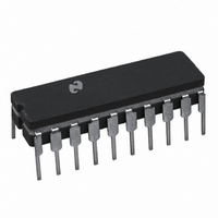
IC ADC 10BIT MPU COMPAT 20-CDIP
Manufacturer
National Semiconductor
Datasheet
1.ADC1005BCJ-1.pdf
(16 pages)
Specifications of ADC1005BCJ-1
Number Of Bits
10
Data Interface
Parallel
Number Of Converters
1
Voltage Supply Source
Single Supply
Operating Temperature
-40°C ~ 85°C
Mounting Type
Through Hole
Package / Case
20-CDIP (0.300", 7.62mm)
Lead Free Status / RoHS Status
Contains lead / RoHS non-compliant
Other names
*ADC1005BCJ-1
Available stocks
Company
Part Number
Manufacturer
Quantity
Price


set. As long as the CS input and WR input remain low, the A/
D will remain in a reset state. Conversion will start after at
least one of these inputs makes a low-to-high transition.
1.3 Output Control
After the “1” is clocked through the 10-bit shift register (which
completes the SAR search) it causes the new digital word to
transfer to the TRI-STATE output latches. When the XFER
signal makes a high-to-low transition the one shot fires, set-
ting the INTR F/F. An inverting buffer then supplies the
INTR output signal.
Note that this SET control of the INTR F/F remains low for
approximately 400 ns. If the data output is continuously en-
abled (CS and RD both held low) the INTR output will still
signal the end of the conversion (by a high-to-low transition).
This is because the SET input can control the Q output of the
INTR F/F even though the RESET input is constantly at a “1”
level. This INTR output will therefore stay low for the duration
of the SET signal.
When data is to be read, the combination of both CS and
RD being low will cause the INTR F/F to be reset and the TRI-
STATE output latches will be enabled.
1.4 Free-Running and Self-Clocking Modes
For operation in the free-running mode an initializing pulse
should be used, following power-up, to ensure circuit opera-
tion. In this application, the CS input is grounded and the
WR input is tied to the INTR output. This WR and INTR node
should be momentarily forced to logic low following a power-
up cycle to ensure start up.
The clock for the A/D can be derived from the CPU clock or
an external RC can be added to provide self-clocking. The
CLK IN makes use of a Schmitt trigger as shown in
2.
2.0 REFERENCE VOLTAGE
The voltage applied to the reference input of these converters
defines the voltage span of the analog input (the difference
between V
output codes apply. The devices can be used in either ratio-
metric applications or in systems requiring absolute accuracy.
The reference pin must be connected to a voltage source ca-
pable of driving the reference input resistance of typically 4.8
kΩ. This pin is the top of a resistor divider string used for the
successive approximation conversion.
In a ratiometric system
proportional to the voltage used for the A/D reference. This
IN(MAX)
FIGURE 2. Self-Clocking the A/D
and V
(Figure
IN(MIN)
) over which the 1024 possible
3) the analog input voltage is
5261 Version 8 Revision 2
526112
Figure
Print Date/Time: 2009/08/26 22:47:16
9
voltage is typically the system power supply, so the V
can be tied to V
quirements of the system references as the analog input and
A/D reference move together maintaining the same output
code for a given input condition.
For absolute accuracy
varies between very specific voltage limits, the reference pin
can be biased with a time and temperature stable voltage
source. The LM385 and LM336 reference diodes are good
low current devices to use with these converters.
The maximum value of the reference is limited to the V
supply voltage. The minimum value, however, can be small
to allow direct conversions of transducer outputs providing
less than a 5V output span. Particular care must be taken with
regard to noise pickup, circuit layout, and system error voltage
sources when operating with a reduced span due to the in-
creased sensitivity of the converter (1 LSB equals V
1024).
FIGURE 4. Absolute with a Reduced Span
CC
FIGURE 3. Ratiometric
. This technique relaxes the stability re-
(Figure
4), where the analog input
526117
www.national.com
526118
REF
REF
pin
CC
/
Related parts for ADC1005BCJ-1
Image
Part Number
Description
Manufacturer
Datasheet
Request
R

Part Number:
Description:
ADC1005 - 10-Bit Microprocessor Compatible A/D Converter, Package: Cerdip, Pin Nb=20
Manufacturer:
National Semiconductor Corporation
Datasheet:

Part Number:
Description:
National Semiconductor [8-Bit D/A Converter]
Manufacturer:
National Semiconductor
Datasheet:
Part Number:
Description:
National Semiconductor [Media Coprocessor]
Manufacturer:
National Semiconductor
Datasheet:
Part Number:
Description:
Digitally Controlled Tone and Volume Circuit with Stereo Audio Power Amplifier, Microphone Preamp Stage and National 3D Sound
Manufacturer:
National Semiconductor
Datasheet:
Part Number:
Description:
Digitally Controlled Tone and Volume Circuit with Stereo Audio Power Amplifier, Microphone Preamp Stage and National 3D Sound
Manufacturer:
National Semiconductor
Datasheet:
Part Number:
Description:
AC97 Rev 2 Codec with Sample Rate Conversion and National 3D Sound
Manufacturer:
National Semiconductor
Part Number:
Description:
Manufacturer:
National Semiconductor
Datasheet:
Part Number:
Description:
Manufacturer:
National Semiconductor
Datasheet:
Part Number:
Description:
General Purpose, Low Voltage, Low Power, Rail-to-Rail Output Operational Amplifiers
Manufacturer:
National Semiconductor
Datasheet:
Part Number:
Description:
8-bit 20 MSPS flash A/D converter.
Manufacturer:
National Semiconductor
Datasheet:
Part Number:
Description:
Low Noise Quad Operational Amplifier
Manufacturer:
National Semiconductor
Datasheet:
Part Number:
Description:
Quad Differential Line Receivers
Manufacturer:
National Semiconductor
Datasheet:
Part Number:
Description:
Quad High Speed Trapezoidal? Bus Transceiver
Manufacturer:
National Semiconductor
Datasheet:
Part Number:
Description:
Dual Line Receiver
Manufacturer:
National Semiconductor
Datasheet: