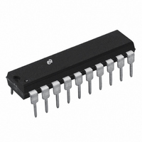
ADC08061CIN National Semiconductor, ADC08061CIN Datasheet - Page 3

ADC08061CIN
Manufacturer Part Number
ADC08061CIN
Description
IC CONVERTER 500 NS A/D 20-DIP
Manufacturer
National Semiconductor
Datasheet
1.ADC08061CIN.pdf
(16 pages)
Specifications of ADC08061CIN
Number Of Bits
8
Sampling Rate (per Second)
300k
Number Of Converters
1
Power Dissipation (max)
100mW
Voltage Supply Source
Single Supply
Operating Temperature
-40°C ~ 85°C
Mounting Type
Through Hole
Package / Case
20-DIP (0.300", 7.62mm)
Lead Free Status / RoHS Status
Contains lead / RoHS non-compliant
Other names
*ADC08061CIN
Available stocks
Company
Part Number
Manufacturer
Quantity
Price
Symbol
t
t
t
t
t
t
t
t
t
t
t
t
t
t
t
t
t
t
t
t
t
C
C
C
WR
RD
RDW
CONV
CRD
ACCO
ACC1
ACC2
0H
1H
INTL
INTH
INTH
RDY
ID
RI
N
AH
AS
CSS
CSH
VIN
OUT
IN
AC Electrical Characteristics
The following specifications apply for V
Boldface limits apply for T
Write Time
Read Time (Time from Falling Edge Mode Pin to V
of WR to Falling Edge of RD)
RD Width
WR-RD Mode Conversion Time
(t
RD Mode Conversion Time
Access Time (Delay from Falling
Edge of RD to Output Valid)
Access Time (Delay from
Falling Edge
of RD to Output Valid)
Access Time (Delay from
Falling Edge
of RD to Output Valid)
TRI-STATE Control (Delay from
Rising Edge of RD to HI-Z State)
TRI-STATE Control (Delay from
Rising Edge of RD to HI-Z State)
Delay from Rising Edge of
WR to Falling Edge of INT
Delay from Rising Edge of
RD to Rising Edge of INT
Delay from Rising Edge of
WR to Rising Edge of INT
Delay from CS to RDY
Delay from INT to Output Valid
Delay from RD to INT
Time between End of RD
and Start of New Conversion
Channel Address Hold Time
Channel Address Setup Time
CS Setup Time
CS Hold Time
Analog Input Capacitance
Logic Output Capacitance
Logic Input Capacitance
WR
a
t
RD
Parameter
a
t
ACC1
)
A
e
T
J
a
e
(Figure 2a)
2b and 4 )
(Figure 3)
(Figure 2a)
Mode Pin to V
( Figures 2a 2b and 3 )
Mode Pin to GND (Figure 4)
Mode Pin to V
Mode Pin to GND (Figure 1)
C
Mode Pin to GND (Figure 1)
C
C
Mode Pin to V
C
C
t
R
R
( Figures 2b and 3 )
Mode Pin
C
C
Mode Pin
R
R
Mode Pin
( Figures 1 2a 2b 3 and 4 )
( Figures 1 2a 2b 3 and 4 )
( Figures 1 2a 2b 3 and 4 )
( Figures 1 2a 2b 3 and 4 )
( Figures 1 2a 2b 3 and 4 )
RD l
e
L s
L s
L
L s
L
L
L
L
L
L
L
T
e
e
e
e
e
e
e
e
MIN
5V t
100 pF
10 pF
10 pF
100 pF
100 pF
3 k
3 k
50 pF ( Figures 1 2a
50 pF (Figure 3)
3 k (Figure 1)
3 k
t
INTL
to T
r
e
e
e
Condition
e
C
C
C
( Figures 2b and 4 )
MAX
V
0V C
V
L
L
L
a
a
a
a
t
a
a
f
e
e
e
e
(Figure 2a)
(Figure 2a)
t
C
t
RD s
10 pF
10 pF
100 pF
RD s
L
L
all other limits T
10 ns V
e
e
3
50 pF
50 pF
t
t
INTL
INTL
REF
(Note 7)
Typical
a
100
350
200
400
500
655
640
520
45
50
25
30
30
30
50
45
25
60
50
10
25
e
A
0
0
0
0
5
5
e
5V V
T
ADC08062 with BIN
J
BIWM CIN and
e
CIWM suffixes
REF
AD08061 and
25 C
(Note 8)
b
Limits
100
350
250
400
560
900
900
110
690
115
55
60
60
95
95
45
15
50
60
0
0
0
e
0V unless otherwise specified
ADC08061CMJ
(Note 8)
(Limit)
http
100
515
250
400
790
940
940
175
690
100
100
175
60
60
60
50
15
50
60
0
0
0
www national com
ns (max)
ns (max)
ns (max)
ns (max)
ns (max)
ns (max)
ns (max)
ns (max)
ns (max)
ns (max)
ns (max)
ns (max)
ns (max)
ns (max)
ns (max)
ns (max)
ns (min)
ns (min)
ns (min)
ns (min)
ns (min)
ns (min)
(Limit)
Units
pF
pF
pF


