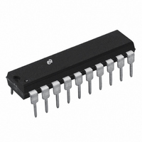
ADC08238CIN National Semiconductor, ADC08238CIN Datasheet - Page 15

ADC08238CIN
Manufacturer Part Number
ADC08238CIN
Description
IC ADC 8BIT NS SERIAL I/O 20-DIP
Manufacturer
National Semiconductor
Datasheet
1.ADC08231BIN.pdf
(24 pages)
Specifications of ADC08238CIN
Number Of Bits
8
Sampling Rate (per Second)
286k
Data Interface
NSC MICROWIRE™, Serial
Number Of Converters
1
Power Dissipation (max)
20mW
Voltage Supply Source
Single Supply
Operating Temperature
-40°C ~ 85°C
Mounting Type
Through Hole
Package / Case
20-DIP (0.300", 7.62mm)
Lead Free Status / RoHS Status
Contains lead / RoHS non-compliant
Other names
*ADC08238CIN
ure 1 illustrates the input flexibility which can be achieved
Functional Description
Since the input configuration is under software control it
can be modified as required before each conversion A
channel can be treated as a single-ended ground refer-
enced input for one conversion then it can be reconfigured
as part of a differential channel for another conversion Fig-
The analog input voltages for each channel can range from
50mV below ground to 50mV above V
out degrading conversion accuracy
2 0 THE DIGITAL INTERFACE
A most important characteristic of these converters is their
serial data link with the controlling processor Using a serial
communication format offers two very significant system im-
provements it allows many functions to be included in a
small package and it can eliminate the transmission of low
level analog signals by locating the converter right at the
analog sensor transmitting highly noise immune digital data
back to the host processor
FIGURE 1 Analog Input Multiplexer Options for the ADC08238
8 Single-Ended
4 Differential
CC
(Continued)
(typically 5V) with-
15
To understand the operation of these converters it is best to
refer to the Timing Diagrams and Functional Block Diagram
and to follow a complete conversion sequence For clarity a
separate timing diagram is shown for each device
1 A conversion is initiated by pulling the CS (chip select)
2 On each rising edge of the clock the status of the data in
line low This line must be held low for the entire conver-
sion The converter is now waiting for a start bit and its
MUX assignment word
(DI) line is clocked into the MUX address shift register
The start bit is the first logic ‘‘1’’ that appears on this line
(all leading zeros are ignored) Following the start bit the
converter expects the next 2 to 4 bits to be the MUX
assignment word
8 Pseudo-Differential
Mixed Mode
TL H 11015 – 17


