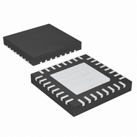
MAX15501GTJ+ Maxim Integrated Products, MAX15501GTJ+ Datasheet - Page 14

MAX15501GTJ+
Manufacturer Part Number
MAX15501GTJ+
Description
IC COND ANLG OUTPUT 2.5V 32-TQFN
Manufacturer
Maxim Integrated Products
Type
Conditionerr
Datasheet
1.MAX15500GTJ.pdf
(28 pages)
Specifications of MAX15501GTJ+
Data Interface
Serial, SPI™
Voltage Supply Source
Analog and Digital
Operating Temperature
-40°C ~ 105°C
Mounting Type
Surface Mount
Package / Case
32-TQFN Exposed Pad
Interface Type
SPI
Supply Voltage (max)
32.5 V
Supply Voltage (min)
15 V
Maximum Operating Temperature
+ 105 C
Minimum Operating Temperature
- 40 C
Mounting Style
SMD/SMT
Lead Free Status / RoHS Status
Lead free / RoHS Compliant
Voltage - Supply
-
Sampling Rate (per Second)
-
Resolution (bits)
-
Lead Free Status / Rohs Status
Lead free / RoHS Compliant
Industrial Analog Current/
Voltage-Output Conditioners
14
_____________________________________________________________________________________
PIN
19
20
21
22
23
25
26
28
29
30
31
—
SENSERN
SENSERP
SENSEVN
SENSEVP
AVDDO
NAME
AVDD
AVSS
MON
OUT
CS1
CS2
EP
Analog Output. The analog voltage or current output range at OUT is programmable. See Tables
1 to 4 for possible output range settings.
Positive Output Driver Supply Voltage Input. AVDDO provides power to the driver output stage.
Bypass AVDDO to AVDD with a 0.1FF capacitor. Use diodes as shown in the Typical Operating
Circuit/Functional Diagram to ensure a voltage difference of 2V to 3.5V between AVDD and
AVDDO.
Sense Resistor Positive Connection. See the Typical Operating Circuit/Functional Diagram for the
typical connection.
Sense Resistor Negative Connection. See the Typical Operating Circuit/Functional Diagram for the
typical connection.
Kelvin Sense Voltage Negative Input. See the Typical Operating Circuit/Functional Diagram for the
typical connection.
Kelvin Sense Voltage Positive Input. See the Typical Operating Circuit/Functional Diagram for the
typical connection.
Positive Analog Supply Voltage Input. Bypass AVDD to AGND with a 0.1FF capacitor.
Negative Analog Supply Voltage Input. Bypass AVSS to AGND with a 0.1FF capacitor.
Load Monitoring Output. MON provides an analog 0 to 3V output. See the Output Monitor section.
Active-Low SPI Chip-Select Input 1. See the SPI Interface section.
Active-Low SPI Chip-Select Input 2. See the SPI Interface section.
Exposed Pad. Internally connected to AVSS. Connect to AVSS. Connect to a large copper area to
maximize thermal performance. Do not connect ground or signal lines through EP.
FUNCTION
Pin Description (continued)


