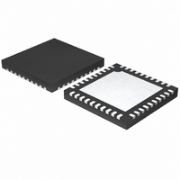
MAX1358BETL+ Maxim Integrated Products, MAX1358BETL+ Datasheet - Page 25

MAX1358BETL+
Manufacturer Part Number
MAX1358BETL+
Description
IC DAS 16BIT 40-TQFN
Manufacturer
Maxim Integrated Products
Type
Data Acquisition System (DAS)r
Datasheet
1.MAX1358BETL.pdf
(71 pages)
Specifications of MAX1358BETL+
Resolution (bits)
16 b
Sampling Rate (per Second)
21.84k
Data Interface
Serial
Voltage Supply Source
Analog and Digital
Voltage - Supply
1.8 V ~ 3.6 V
Operating Temperature
-40°C ~ 85°C
Mounting Type
Surface Mount
Package / Case
40-TQFN Exposed Pad
Number Of Converters
2
Resolution
16 bit
Interface Type
Serial (4-Wire, SPI, QSPI, Microwire)
Voltage Reference
1.25 V
Supply Voltage (max)
3.6 V
Supply Voltage (min)
1.8 V
Maximum Power Dissipation
2051.3 mW
Maximum Operating Temperature
+ 85 C
Mounting Style
SMD/SMT
Input Voltage
1.8 V to 3.6 V
Minimum Operating Temperature
- 40 C
Lead Free Status / RoHS Status
Lead free / RoHS Compliant
16-Bit, Data-Acquisition System with ADC, DACs,
UPIOs, RTC, Voltage Monitors, and Temp Sensor
PIN
23
24
25
26
27
28
29
30
31
32
33
34
35
36
37
38
39
40
—
CPOUT
NAME
AGND
DGND
UPIO1
OUTA
OUTB
DV
AV
SWA
SWB
AIN2
AIN1
REG
FBA
FBB
REF
CF+
CF-
EP
DD
DD
______________________________________________________________________________________
DACA SPST Shunt Switch Input. Connects to OUTA through an SPST switch.
DACA Force-Sense Feedback Input. Analog input to mux.
DACA Force-Sense Output. Analog input to mux.
Analog Ground
Analog Supply Voltage. Also ADC reference voltage during AV
10μF and 0.1μF capacitors in parallel as close to the pin as possible.
DACB SPST Shunt Switch Input. Connects to OUTB through an SPST switch.
DACB Force-Sense Feedback Input. Analog input to mux.
Force-Sense DACB Ouput. Analog input to mux.
Analog Input 2. Analog input to mux. Inputs have internal programmable current source for external
temperature measurement.
Analog Input 1. Analog input to mux. Inputs have internal programmable current source for external
temperature measurement.
Reference Input/Output. Output of the reference buffer amplifier or external reference input. Disabled at
power-up to allow external reference. Reference voltage for ADC and DACs.
Linear Voltage-Regulator Output. Charge-pump-doubler input voltage. Bypass REG with a 10μF capacitor
to DGND for charge-pump regulation.
Charge-Pump Flying Capacitor Terminals. Connect an external 10μF (typ) capacitor between CF+ and CF-.
Charge-Pump Output. Connect an external 10μF (typ) reservoir capacitor between CPOUT and DGND. There is
a low threshold diode between DV
within 300mV (typ) of DV
Digital Supply Voltage. Bypass to DGND with 10μF and 0.1μF capacitors in parallel as close to the pin as
possible.
Digital Ground. Also ground for cascaded linear voltage regulator and charge-pump doubler.
User-Programmable Input/Output 1. See the UPIO1_CTRL Register for functionality.
Exposed Pad. Leave unconnected or connect to AGND.
DD
.
DD
and CPOUT. When the charge pump is disabled, CPOUT is pulled up
FUNCTION
Pin Description (continued)
DD
measurement. Bypass to AGND with
25


