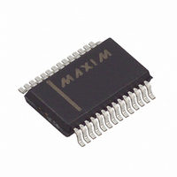
MAX128BCAI+ Maxim Integrated Products, MAX128BCAI+ Datasheet - Page 13

MAX128BCAI+
Manufacturer Part Number
MAX128BCAI+
Description
IC DAS 12BIT 2-WIRE 28-SSOP
Manufacturer
Maxim Integrated Products
Type
Data Acquisition System (DAS)r
Datasheet
1.MAX128BCAI.pdf
(16 pages)
Specifications of MAX128BCAI+
Resolution (bits)
12 b
Sampling Rate (per Second)
8k
Data Interface
Serial
Voltage Supply Source
Single Supply
Voltage - Supply
4.75 V ~ 5.25 V
Operating Temperature
0°C ~ 70°C
Mounting Type
Surface Mount
Package / Case
28-SSOP
Lead Free Status / RoHS Status
Lead free / RoHS Compliant
Figure 10. Complete 2-Wire Serial Read Transmission
The MAX127/MAX128 ignore acknowledge and NOT-
acknowledge conditions issued by the master during
the read cycle. The device waits for the master to read
the output data or waits until a STOP condition is
issued. Figure 10 shows a complete read cycle.
In unipolar input mode, the output is straight binary. For
bipolar input mode, the output is two’s complement. For
output binary codes see the Transfer Function section.
The MAX127/MAX128 power up in normal operating
mode, waiting for a START condition followed by the
appropriate slave address. The contents of the input
and output data registers are cleared at power-up.
The MAX127/MAX128 operate with either an internal or
an external reference (Figures 11a–11c). An external
reference is connected to either REF or to REFADJ.
The REFADJ internal buffer gain is trimmed to 1.6384 to
provide 4.096V at REF from a 2.5V reference.
The internally trimmed 2.50V reference is amplified
through the REFADJ buffer to provide 4.096V at REF.
Bypass REF with a 4.7µF capacitor to AGND and bypass
REFADJ with a 0.01µF capacitor to AGND (Figure 11a).
The internal reference voltage is adjustable to ±1.5%
(±65 LSBs) with the reference-adjust circuit of Figure 12.
CONDITION
START
Applications Information
Internal or External Reference
MSB
1
0
______________________________________________________________________________________
SLAVE ADDRESS BYTE
1
2
7
LSB
Power-On Reset
R
8
Internal Reference
Multirange, +5V, 12-Bit DAS with
A
9
MSB
D11
10
MSB DATA BYTE
11
LSB
D4
17
To use the REF input directly, disable the internal buffer
by connecting REFADJ to V
REFADJ input eliminates the need to buffer the refer-
ence externally. When the reference is applied at
REFADJ, bypass REFADJ with a 0.01µF capacitor to
AGND (Figure 11c).
At REF and REFADJ, the input impedance is a mini-
mum of 10kΩ for DC currents. During conversions, an
external reference at REF must be able to drive a
400µA DC load, and must have an output impedance
of 10Ω or less. If the reference has higher input imped-
ance or is noisy, bypass REF with a 4.7µF capacitor to
AGND as close to the chip as possible.
With an external reference voltage of less than 4.096V
at REF or less than 2.5V at REFADJ, the increase in
RMS noise to the LSB value (full-scale voltage/4096)
results in performance degradation and loss of effec-
tive bits.
To save power, put the converter into low-current shut-
down mode between conversions. Two programmable
power-down modes are available, in addition to the
hardware shutdown. Select STBYPD or FULLPD by pro-
gramming PD0 and PD1 in the input control byte (Table
4). When software power-down is asserted, it becomes
effective only after the end of conversion. In all power-
down modes, the interface remains active and conver-
sion results may be read. Input overvoltage protection
is active in all power-down modes.
2-Wire Serial Interface
A
18
MSB
D3
19
LSB DATA BYTE
22
D0
23
FILLED WITH
4 ZEROS
DD
LSB
26
Power-Down Mode
(Figure 11b). Using the
27
A
External Reference
CONDITION
STOP
13


