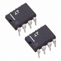
LTC1091CN8 Linear Technology, LTC1091CN8 Datasheet - Page 18

LTC1091CN8
Manufacturer Part Number
LTC1091CN8
Description
IC DATA ACQ SYS 10BIT 2CH 8-DIP
Manufacturer
Linear Technology
Type
Data Acquisition System (DAS), ADCr
Datasheet
1.LTC1091CN8PBF.pdf
(32 pages)
Specifications of LTC1091CN8
Resolution (bits)
10 b
Data Interface
Serial
Voltage Supply Source
Single Supply
Voltage - Supply
4.5 V ~ 10 V
Operating Temperature
-40°C ~ 85°C
Mounting Type
Through Hole
Package / Case
8-DIP (0.300", 7.62mm)
Lead Free Status / RoHS Status
Contains lead / RoHS non-compliant
Sampling Rate (per Second)
-
Available stocks
Company
Part Number
Manufacturer
Quantity
Price
Company:
Part Number:
LTC1091CN8
Manufacturer:
LT
Quantity:
5 510
Company:
Part Number:
LTC1091CN8
Manufacturer:
NSMDA
Quantity:
5 510
Part Number:
LTC1091CN8
Manufacturer:
LT/凌特
Quantity:
20 000
Part Number:
LTC1091CN8#PBF
Manufacturer:
LINEAR/凌特
Quantity:
20 000
Motorola SPI (MC68HC05C4, MC68HC11)
The MC68HC05C4 has been chosen as an example of an
MPU with a dedicated serial port. This MPU transfers data
MSB first and in 8-bit increments. With two 8-bit transfers,
the A/D result is read into the MPU. The first 8-bit transfer
sends the D
of the A/D conversion result into the processor. The
ANALOG
18
LTC1091/LTC1092
LTC1093/LTC1094
A
INPUTS
PPLICATI
LOCATION A + 1
D
MPU TRANSMIT
LOCATION A
MPU RECEIVED
OUT
from LTC1091 Stored in MC68HC05C4 RAM
IN
WORD
WORD
Hardware and Software Interface to
D
Motorola MC68HC05C4 Processor
LTC1091
word to the LTC1091 and clocks B9 and B8
CLK
OUT
D
CS
IN
0
B7
O
D OUT
U
0
B6
CLK
D IN
CS
S
0
B5
0
?
I FOR ATIO
U
0
B4
START
START
BIT
1
?
0
B3
SGL/
DIFF
SGL/
DIFF
?
0
B2
Data Exchange Between LTC1091 and MC68HC05C4
1ST TRANSFER
MSB
W
ODD/
SIGN
ODD/
B9
SIGN
CO
SCK
MOSI
MISO
B1
?
BYTE 1
BYTE 1
LSB
MSBF
MSBF
B8
B0
MC68HC05C4
?
1091-4 AI16
BYTE 1
BYTE 2
X
0
U
B9
B9
X
B8
X
B8
second 8-bit transfer clocks the remaining bits, B7 through
B0, into the MPU.
ANDing the first MPU received byte with 03 Hex clears the
six most significant bits. Notice how the position of the
start bit in the first MPU transmit word is used to position
the A/D result right justified in two memory locations.
LABEL
START
B7
X
B7
DON’T CARE
B6
X
MNEMONIC
BCLRn
LDA
STA
TST
BPL
LDA
STA
AND
STA
TST
BPL
BSETn
LDA
STA
B6
B5
X
B5
BYTE 2 (DUMMY)
2ND TRANSFER
B4
X = DON’T CARE
X
BYTE 2
B4
COMMENTS
Bit 0 Port C Goes Low (CS Goes Low)
Load LTC1090 D
Load LTC1090 D
Transfer Begins
Test Status of SPIF
Loop to Previous Instruction If Not Done
with Transfer
Load contents of SPI Data Register into
Acc (D
Start Next SPI Cycle
Clear 6 MSBs of First D
Store in Memory Location A (MSBs)
Test Status of SPIF
Loop to Previous Instruction If Not Done
with Transfer
Set B0 of Port C (CS Goes High)
Load contents of SPI Data Register into
Acc (D
Store in Memory location A + 1 (LSBs)
B3
X
B3
B2
OUT
OUT
X
B2
MSBs)
LSBs)
B1
X
B1
IN
IN
B0
X
B0
Word into Acc
Word into SPI from Acc
OUT
1091/2/3/4 AI15
Word


