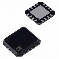
AD7879-1ACPZ-RL Analog Devices Inc, AD7879-1ACPZ-RL Datasheet - Page 8

AD7879-1ACPZ-RL
Manufacturer Part Number
AD7879-1ACPZ-RL
Description
IC ADC 12BIT CTLR TOUCH 16LFCSP
Manufacturer
Analog Devices Inc
Type
Resistiver
Specifications of AD7879-1ACPZ-RL
Resolution (bits)
12 b
Data Interface
I²C, Serial
Touch Panel Interface
4-Wire
Number Of Inputs/keys
1 TSC
Data Rate/sampling Rate (sps, Bps)
105k
Voltage Reference
External
Voltage - Supply
1.6 V ~ 3.6 V
Current - Supply
10nA
Operating Temperature
-40°C ~ 85°C
Mounting Type
Surface Mount
Package / Case
16-LFCSP
Voltage Supply Source
Single Supply
Sampling Rate (per Second)
105k
Sampling Rate
105kSPS
Supply Voltage Range - Analog
1.6V To 3.6V
Supply Current
480µA
Digital Ic Case Style
CSP
No. Of Pins
16
Lead Free Status / RoHS Status
Lead free / RoHS Compliant
AD7879/AD7889
Table 7. Pin Function Descriptions, LFCSP
AD7879
1
2, 3, 10, 11
4
5
6
N/A
7
8
9
N/A
12
13
14
N/A
15
16
NOTES
1. NC = NO CONNECT
2. THE EXPOSED PAD IS NOT CONNECTED INTERNALLY.
AND MAXIMUM THERMAL CAPABILITY, IT IS RECOMMENDED
FOR INCREASED RELIABILITY OF THE SOLDER JOINTS
THAT THE PAD BE SOLDERED TO THE GROUND PLANE.
Pin No.
NC
NC
Y+
X–
AD7879-1
1
2, 3, 10, 11
4
5
N/A
6
7
8
N/A
9
12
13
N/A
14
15
16
Figure 7. AD7879 LFCSP Pin Configuration
1
2
3
4
(Not to Scale)
AD7879
TOP VIEW
PIN 1
INDICATOR
Mnemonic
Y+
NC
X−
Y−
DIN
ADD1
GND
SCL
DOUT
SDA
PENIRQ/INT/DAV
AUX/VBAT/GPIO
CS
ADD0
V
X+
EP
CC
/REF
12
11 NC
10 NC
9 DOUT
PENIRQ/INT/DAV
Description
Touch Screen Input Channel.
No Connect.
Touch Screen Input Channel.
Touch Screen Input Channel.
SPI Serial Data Input to the AD7879.
I
for the AD7879-1 (see Table 25).
Ground. Ground reference point for all circuitry on the AD7879. All analog input signals and
any external reference signal should be referred to this voltage.
Serial Interface Clock Input.
SPI Serial Data Output for the AD7879.
I
Interrupt Output. This pin is asserted when the screen is touched (PENIRQ), when a measure-
ment exceeds the preprogrammed limits (INT), or when new data is available in the registers
(DAV). Active low, internal 50 kΩ pull-up resistor.
This pin can be programmed as an auxiliary input to the ADC (AUX), as a battery measure-
ment input to the ADC (VBAT), or as a general-purpose digital input/output (GPIO).
Chip Select for the SPI Serial Interface on the AD7879. Active low.
I
for the AD7879-1 (see Table 25).
Power Supply Input and ADC Reference.
Touch Screen Input Channel.
Exposed Pad. The exposed pad is not connected internally. For increased reliability of the
solder joints and maximum thermal capability, it is recommended that the pad be soldered
to the ground plane.
2
2
2
C Address Bit 1 for the AD7879-1. This pin can be tied high or low to determine an address
C Serial Data Input and Output for the AD7879-1.
C Address Bit 0 for the AD7879-1. This pin can be tied high or low to determine an address
Rev. C | Page 8 of 40
NOTES
1. NC = NO CONNECT
2. THE EXPOSED PAD IS NOT CONNECTED INTERNALLY.
AND MAXIMUM THERMAL CAPABILITY, IT IS RECOMMENDED
FOR INCREASED RELIABILITY OF THE SOLDER JOINTS
THAT THE PAD BE SOLDERED TO THE GROUND PLANE.
Figure 8. AD7879-1 LFCSP Pin Configuration
NC
NC
Y+
X–
1
2
3
4
(Not to Scale)
AD7879-1
TOP VIEW
PIN 1
INDICATOR
12
11 NC
10 NC
9 SDA
PENIRQ/INT/DAV


