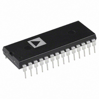
AD7874ANZ Analog Devices Inc, AD7874ANZ Datasheet - Page 6

AD7874ANZ
Manufacturer Part Number
AD7874ANZ
Description
IC DAS 12BIT 4CH LC2MOS 28-DIP
Manufacturer
Analog Devices Inc
Type
Data Acquisition System (DAS)r
Datasheet
1.AD7874ARZ.pdf
(16 pages)
Specifications of AD7874ANZ
Resolution (bits)
12 b
Data Interface
Parallel
Sampling Rate (per Second)
116k
Voltage Supply Source
Dual ±
Voltage - Supply
5V
Operating Temperature
-40°C ~ 85°C
Mounting Type
Through Hole
Package / Case
28-DIP (0.600", 15.24mm)
Sampling Rate
116kSPS
Input Channel Type
Single Ended
Supply Voltage Range - Analog
± 4.75V To ± 5.25V
Supply Current
12mA
Lead Free Status / RoHS Status
Lead free / RoHS Compliant
Available stocks
Company
Part Number
Manufacturer
Quantity
Price
Company:
Part Number:
AD7874ANZ
Manufacturer:
AD
Quantity:
5 530
AD7874
CONVERTER DETAILS
The AD7874 is a complete 12-bit, 4-channel data acquisition
system. It is comprised of a 12-bit successive approximation
ADC, four high speed track/hold circuits, a four-channel analog
multiplexer and a 3 V Zener reference. The ADC uses a succes-
sive approximation technique and is based on a fast-settling,
voltage switching DAC, a high speed comparator, a fast CMOS
SAR and high speed logic.
Conversion is initiated on the rising edge of CONVST. All four
input track/holds go from track to hold on this edge. Conversion
is first performed on the Channel 1 input voltage, then Channel
2 is converted and so on. The four results are stored in on-chip
registers. When all four conversions have been completed, INT
goes low indicating that data can be read from these locations.
The conversion sequence takes either 78 or 79 rising clock edges
depending on the synchronization of CONVST with CLK. In-
ternal delays and reset times bring the total conversion time
from CONVST going high to INT going low to 32.5 s maxi-
mum for a 2.5 MHz external clock. The AD7874 uses an im-
plicit addressing scheme whereby four successive reads to the
same memory location access the four data words sequentially.
The first read accesses Channel 1 data, the second read accesses
Channel 2 data and so on. Individual data registers cannot be
accessed independently.
INTERNAL REFERENCE
The AD7874 has an on-chip temperature compensated buried
Zener reference which is factory trimmed to 3 V
Figure 3). The reference voltage is provided at the REF OUT
pin. This reference can be used to provide both the reference
voltage for the ADC and the bipolar bias circuitry. This is
achieved by connecting REF OUT to REF IN.
The reference can also be used as a reference for other compo-
nents and is capable of providing up to 500 A to an external
load. In systems using several AD7874s, using the REF OUT of
one device to provide the REF IN for the other devices ensures
good full-scale tracking between all the AD7874s. Because the
AD7874 REF IN is buffered, each AD7874 presents a high im-
pedance to the reference so one AD7874 REF OUT can drive
several AD7874 REF INs.
The maximum recommended capacitance on REF OUT for
normal operation is 50 pF. If the reference is required for other
system uses, it should be decoupled to AGND with a 200
sistor in series with a parallel combination of a 10 F tantalum
capacitor and a 0.1 F ceramic capacitor.
Figure 3. AD7874 Internal Reference
V
V
DD
SS
COMPENSATION
TEMPERATURE
AD7874
REF OUT
10 mV (see
re-
–6–
EXTERNAL REFERENCE
In some applications, the user may require a system reference or
some other external reference to drive the AD7874 reference in-
put. Figure 4 shows how the AD586 5 V reference can be used
to provide the 3 V reference required by the AD7874 REF IN.
TRACK-AND-HOLD AMPLIFIER
The track-and-hold amplifier on each analog input of the
AD7874 allows the ADC to accurately convert an input sine
wave of 20 V p-p amplitude to 12-bit accuracy. The input band-
width of the track/hold amplifier is greater than the Nyquist rate
of the ADC even when the ADC is operated at its maximum
throughput rate. The small signal 3 dB cutoff frequency occurs
typically at 500 kHz.
The four track/hold amplifiers sample their respective input
channels simultaneously. The aperture delay of the track/hold
circuits is small and, more importantly, is well matched across
the four track/holds on one device and also well matched from
device to device. This allows the relative phase information be-
tween different input channels to be accurately preserved. It also
allows multiple AD7874s to sample more than four channels
simultaneously.
The operation of the track/hold amplifiers is essentially transpar-
ent to the user. Once conversion is initiated, the four channels
are automatically converted and there is no need to select which
channel is to be digitized.
ANALOG INPUT
The analog input of Channel 1 of the AD7874 is as shown in
Figure 4. The analog input range is 10 V into an input resis-
tance of typically 30 k . The designed code transitions occur
midway between successive integer LSB values (i.e., 1/2 LSB,
3/2 LSBs, 5/2 LSBs, . . . FS – 3/2 LSBs). The output code is
2s complement binary with 1 LSB = FS/4096 = 20 V/4096 =
4.88 mV. The ideal input/output transfer function is shown in
Figure 5.
GND
AD586
+
15V
+V
Figure 4. AD586 Driving AD7874 REF IN
IN
V
10k
15k
OUT
1k
AGND
REF
V
IN1
IN
**ADDITIONAL PINS OMITTED FOR CLARITY
*R = 3.6k TYP
7R*
2.1R*
3R*
TRACK/HOLD 1
TO ADC
REFERENCE
CIRCUITRY
AD7874**
TO INTERNAL
COMPARATOR
REV. C


