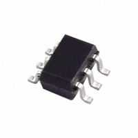
AD5246BKSZ10-RL7 Analog Devices Inc, AD5246BKSZ10-RL7 Datasheet - Page 12

AD5246BKSZ10-RL7
Manufacturer Part Number
AD5246BKSZ10-RL7
Description
IC POT DGTL RES 128POS SC70-6
Manufacturer
Analog Devices Inc
Datasheet
1.AD5246BKSZ50-RL7.pdf
(16 pages)
Specifications of AD5246BKSZ10-RL7
Taps
128
Resistance (ohms)
10K
Number Of Circuits
1
Temperature Coefficient
45 ppm/°C Typical
Memory Type
Volatile
Interface
I²C, 2-Wire Serial
Voltage - Supply
2.7 V ~ 5.5 V
Operating Temperature
-40°C ~ 125°C
Mounting Type
Surface Mount
Package / Case
SC-70-6, SC-88, SOT-363
Resistance In Ohms
10K
End To End Resistance
10kohm
Track Taper
Linear
No. Of Steps
128
Resistance Tolerance
± 20%
Supply Voltage Range
2.7V To 5.5V
Control Interface
I2C, Serial
No. Of Pots
Single
Number Of Elements
1
# Of Taps
128
Resistance (max)
10KOhm
Power Supply Requirement
Single
Interface Type
Serial (2-Wire/I2C)
Single Supply Voltage (typ)
3/5V
Dual Supply Voltage (typ)
Not RequiredV
Single Supply Voltage (min)
2.7V
Single Supply Voltage (max)
5.5V
Dual Supply Voltage (min)
Not RequiredV
Dual Supply Voltage (max)
Not RequiredV
Operating Temp Range
-40C to 125C
Operating Temperature Classification
Automotive
Mounting
Surface Mount
Pin Count
6
Package Type
SC-70
Lead Free Status / RoHS Status
Lead free / RoHS Compliant
Lead Free Status / RoHS Status
Lead free / RoHS Compliant, Lead free / RoHS Compliant
Other names
AD5246BKSZ10-RL7
AD5246BKSZ10-RL7TR
AD5246BKSZ10-RL7TR
AD5246
I
Table 6. Write Mode
S
Table 7. Read Mode
S
S = Start Condition.
P = Stop Condition.
A = Acknowledge.
X = Don’t Care.
2
C INTERFACE
SDA
SCL
0
0
P
t
START BY
START BY
1
1
1
MASTER
MASTER
S
Slave Address Byte
0
0
SCL
SDA
Slave Address Byte
SDA
t
SCL
2
1
1
1
0
1
0
t
SLAVE ADDRESS BYTE
3
1
1
1
1
SLAVE ADDRESS BYTE
FRAME 1
0
t
0
8
t
8
1
1
FRAME 1
1
1
t
9
Figure 26. I
1
1
0
0
Figure 28. Reading from the RDAC Register
Figure 27. Writing to the RDAC Register
t
1
1
6
2
W
R
0
C Interface, Detailed Timing Diagram
0
t
t
4
9
Rev. B | Page 12 of 16
R/W
R/W
A
A
ACK BY
AD5246
ACK BY
AD5246
9
9
X
X
0
1
0
1
t
7
W = Write.
R = Read.
D6, D5, D4, D3, D2, D1, D0 = Data Bits.
D6
D6
D6
D6
D5
D5
RDAC REGISTER
DATA BYTE
FRAME 2
D4
D4
FRAME 2
S
D5
D5
t
5
D3
D3
D4
D4
Data Byte
Data Byte
D2
D2
t
2
D1
D1
D3
D3
D0
D0
ACK BY
AD5246
NO ACK
BY MASTER
9
D2
D2
9
STOP BY
1
MASTER
STOP BY
MASTER
D1
D1
D0
D0
P
A
A
t
10
P
P


