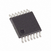
MAX5415EUD+ Maxim Integrated Products, MAX5415EUD+ Datasheet - Page 3

MAX5415EUD+
Manufacturer Part Number
MAX5415EUD+
Description
IC DGTL POT DUAL 256-TAP 14TSSOP
Manufacturer
Maxim Integrated Products
Datasheet
1.MAX5415EUD.pdf
(11 pages)
Specifications of MAX5415EUD+
Taps
256
Resistance (ohms)
100K
Number Of Circuits
2
Temperature Coefficient
35 ppm/°C Typical
Memory Type
Volatile
Interface
SPI, 3-Wire Serial
Voltage - Supply
2.7 V ~ 5.5 V
Operating Temperature
-40°C ~ 85°C
Mounting Type
Surface Mount
Package / Case
14-TSSOP
Resistance In Ohms
100K
Number Of Pots
Dual
Taps Per Pot
256
Resistance
100 KOhms
Wiper Memory
Volatile
Buffered Wiper
Non Buffered
Digital Interface
3-Wire (SPI)
Operating Supply Voltage
2.7 V to 5.5 V
Supply Current
0.8 uA
Maximum Operating Temperature
+ 85 C
Minimum Operating Temperature
- 40 C
Description/function
Dual 256-Tap, Low Drift, Digital Potentiometers in 14-TSSOP
Mounting Style
SMD/SMT
Supply Voltage (max)
5.5 V
Supply Voltage (min)
2.7 V
Tolerance
25 %
Lead Free Status / RoHS Status
Lead free / RoHS Compliant
ELECTRICAL CHARACTERISTICS (continued)
(V
unless otherwise noted.)
Dual, 256-Tap, Low-Drift, Digital Potentiometers
Note 1: Linearity is defined in terms of the H
Note 2: The DNL and INL are measured with the potentiometer configured as a voltage-divider with H
Note 3: The DNL and INL are measured with the potentiometer configured as a variable resistor. H
Note 4: The wiper resistance is the worst value measured by injecting into W
Note 5: Digital timing is guaranteed by design.
DIGITAL INPUTS
Input High Voltage
Input Low Voltage
Input Leakage Current
Input Capacitance
Wiper-Settling Time
TIMING CHARACTERISTICS (DIGITAL) (Note 5)
Maximum SCLK Frequency
SCLK Clock Period
SCLK Pulse Width High
SCLK Pulse Width Low
CS Fall to SCLK Rise Setup Time
SCLK Rise to CS Rise Hold Time
DIN Setup Time
DIN Hold Time
SCLK Rise to CS Fall Delay
CS Rise to SCLK Rise Hold
CS Pulse Width High
POWER SUPPLIES
Supply Voltage
Supply Current
TIMING CHARACTERISTICS (ANALOG)
DD
= +5V, unless otherwise noted. V
terminal is unloaded and measured with an ideal voltmeter.
V
uration, and 40µA for the 100kΩ configuration. At V
respectively.
PARAMETER
DD
= +5V, the wiper terminal is driven with a source current of 400µA for the 10kΩ configuration, 80µA for the 50kΩ config-
_______________________________________________________________________________________
SYMBOL
t
t
t
t
t
V
CSW
V
t
t
CSS
CSH
t
t
I
V
t
CS0
CS1
t
CP
CH
DS
DH
DD
CL
DD
IH
S
IL
H
= V
X
to L
DD
MAX5413
MAX5414
MAX5415
CS = SCLK = DIN = V
X
, V
code-dependent resistance.
L
= 0, T
DD
A
CONDITIONS
= +3V, 200µA/40µA/20µA for 10kΩ/50kΩ/100kΩ configurations,
= T
MIN
DD
to T
X
MAX
V
V
, a current I
DD
DD
. Typical values are at V
= +5V
= +2.7V
in 14-Pin TSSOP
W
= V
0.7 x V
MIN
100
100
2.7
DD
10
40
40
40
40
10
40
0
0
DD
/ R
X
is unconnected and L
HL
X
= V
.
TYP
100
325
650
0.8
0.1
5
DD
DD
and L
= +5V, T
0.3 x V
MAX
±1.0
X
5.5
5
= 0. The wiper
DD
A
X
= +25°C,
= 0. At
UNITS
MHz
µA
µA
µA
pF
ns
ns
ns
ns
ns
ns
ns
ns
ns
ns
ns
V
V
V
3


