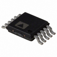
AD5243BRMZ100 Analog Devices Inc, AD5243BRMZ100 Datasheet - Page 7

AD5243BRMZ100
Manufacturer Part Number
AD5243BRMZ100
Description
IC DGTL POT DUAL 100K I2C 10MSOP
Manufacturer
Analog Devices Inc
Datasheet
1.AD5243BRMZ2.5.pdf
(20 pages)
Specifications of AD5243BRMZ100
Temperature Coefficient
35 ppm/°C Typical
Taps
256
Resistance (ohms)
100K
Number Of Circuits
2
Memory Type
Volatile
Interface
I²C, 2-Wire Serial
Voltage - Supply
2.7 V ~ 5.5 V
Operating Temperature
-40°C ~ 125°C
Mounting Type
Surface Mount
Package / Case
10-MSOP, Micro10™, 10-uMAX, 10-uSOP
Resistance In Ohms
100K
End To End Resistance
100kohm
No. Of Steps
256
Resistance Tolerance
± 20%
Supply Voltage Range
2.7V To 5.5V
Control Interface
Serial, I2C, 2-Wire
No. Of Pots
Dual
Number Of Elements
2
# Of Taps
256
Resistance (max)
100KOhm
Power Supply Requirement
Single
Interface Type
Serial (2-Wire/I2C)
Single Supply Voltage (typ)
3/5V
Dual Supply Voltage (typ)
Not RequiredV
Single Supply Voltage (min)
2.7V
Single Supply Voltage (max)
5.5V
Dual Supply Voltage (min)
Not RequiredV
Dual Supply Voltage (max)
Not RequiredV
Operating Temp Range
-40C to 125C
Operating Temperature Classification
Automotive
Mounting
Surface Mount
Pin Count
10
Lead Free Status / RoHS Status
Lead free / RoHS Compliant
For Use With
AD5243EVAL - BOARD EVAL FOR AD5243
Lead Free Status / Rohs Status
Compliant
Available stocks
Company
Part Number
Manufacturer
Quantity
Price
Part Number:
AD5243BRMZ100
Manufacturer:
ADI/亚德诺
Quantity:
20 000
Part Number:
AD5243BRMZ100-RL7
Manufacturer:
ADI/亚德诺
Quantity:
20 000
PIN CONFIGURATIONS AND FUNCTION DESCRIPTIONS
Table 5. AD5243 Pin Function Descriptions
Pin
No.
1
2
3
4
5
6
7
8
9
10
Mnemonic
B1
A1
W2
GND
V
SCL
SDA
A2
B2
W1
DD
Figure 4. AD5243 Pin Configuration
GND
V
W2
B1
A1
DD
Description
B1 Terminal.
A1 Terminal.
W2 Terminal.
Digital Ground.
Positive Power Supply.
Serial Clock Input. Positive-edge
triggered.
Serial Data Input/Output.
A2 Terminal.
B2 Terminal.
W1 Terminal.
1
2
3
4
5
TOP VIEW
AD5243
10
9
8
7
6
W1
B2
A2
SDA
SCL
Rev. A | Page 7 of 20
Table 6. AD5248 Pin Function Descriptions
Pin
No.
1
2
3
4
5
6
7
8
9
10
Mnemonic
B1
AD0
W2
GND
V
SCL
SDA
AD1
B2
W1
DD
Figure 5. AD5248 Pin Configuration
GND
AD0
V
W2
B1
DD
Description
B1 Terminal.
Programmable Address Bit 0 for Multiple
Package Decoding.
W2 Terminal.
Digital Ground.
Positive Power Supply.
Serial Clock Input. Positive-edge
triggered.
Serial Data Input/Output.
Programmable Address Bit 1 for Multiple
Package Decoding.
B2 Terminal.
W1 Terminal.
1
2
3
4
5
TOP VIEW
AD5248
10
9
8
7
6
AD5243/AD5248
W1
B2
AD1
SDA
SCL


