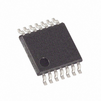
DS1855E-C01+T&R Maxim Integrated Products, DS1855E-C01+T&R Datasheet - Page 4

DS1855E-C01+T&R
Manufacturer Part Number
DS1855E-C01+T&R
Description
IC DUAL NV DGTL POT/MEM 14-TSSOP
Manufacturer
Maxim Integrated Products
Datasheet
1.DS1855E-010.pdf
(20 pages)
Specifications of DS1855E-C01+T&R
Taps
100, 256
Resistance (ohms)
10K
Number Of Circuits
2
Temperature Coefficient
750 ppm/°C Typical
Memory Type
Non-Volatile
Interface
I²C, 2-Wire Serial
Voltage - Supply
2.7 V ~ 5.5 V
Operating Temperature
-40°C ~ 85°C
Mounting Type
Surface Mount
Package / Case
14-TSSOP
Resistance In Ohms
10K
Lead Free Status / RoHS Status
Lead free / RoHS Compliant
MEMORY ORGANIZATION
The DS1855’s serial EEPROM is internally organized with 256 words of 1 byte each. Each word requires
an 8-bit address for random word addressing. The byte at address F9h determines the wiper setting for
potentiometer 0, which contains 100 positions. Writing values above 63h to this address sets the wiper to
its uppermost position, but the MSB is ignored. The byte at address F8h determines the wiper setting for
potentiometer 1, which contains 256 positions (00h to FFh). Address locations FAh though FFh are
reserved and should not be written.
MEMORY
LOCATION
00h – F7h
F8h
F9h
FAh
User Memory
Potentiometer 1 Setting Writing to this byte controls the setting of potentiometer 1, a 256-
Potentiometer 0 Setting Writing to this byte controls the setting of potentiometer 0, a 100-
Software Lock
Configuration Byte
LOCATION
MEMORY
NAME OF
FUNCTION OF MEMORY LOCATION
General-purpose user memory.
position pot. Valid settings are 00h to FFh.
position pot. Valid settings are 00h to 63h. MSB is ignored.
The three lower bits in this byte can be used to set write-protection
to the 256-byte memory block.
B2: Writing this bit to a 1 protects the upper page of memory. If
this bit is set, memory locations F8h to FFh are configured for
write-protection.
B1: Writing this bit to a 1 protects the upper block of memory. If
this bit is set, memory locations 80h to F7h are configured for
write-protection. The upper page must be unlocked in order to
modify the locking of this portion of memory.
B0: Writing this bit to a 1 protects the lower block of memory. If
this bit is set, memory locations 00h to 7Fh are configured for
write-protection. The upper page must be unlocked in order to
modify the locking of this portion of memory.
4 of 4
B2 B1 B0


