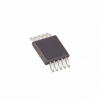
MAX5421CEUB+ Maxim Integrated Products, MAX5421CEUB+ Datasheet - Page 2

MAX5421CEUB+
Manufacturer Part Number
MAX5421CEUB+
Description
IC VOLTAGE DIVIDER DGLT 10MSOP
Manufacturer
Maxim Integrated Products
Datasheet
1.MAX5420AEUA.pdf
(9 pages)
Specifications of MAX5421CEUB+
Taps
4
Resistance (ohms)
15K
Number Of Circuits
1
Memory Type
Volatile
Interface
2-Wire Parallel
Voltage - Supply
4.75 V ~ 5.25 V, ±0.0 V ~ 5.25 V
Operating Temperature
-40°C ~ 85°C
Mounting Type
Surface Mount
Package / Case
10-MSOP, Micro10™, 10-uMAX, 10-uSOP
Resistance In Ohms
15K
Lead Free Status / RoHS Status
Lead free / RoHS Compliant
Temperature Coefficient
-
ABSOLUTE MAXIMUM RATINGS
V
V
D0, D1 to GND ...........................................-0.3V to (V
H, L, W, MATCH_ to GND ................(V
Input and Output Latchup Immunity.................................±50mA
Digitally Programmable Precision
Voltage Divider for PGAs
Stresses beyond those listed under “Absolute Maximum Ratings” may cause permanent damage to the device. These are stress ratings only, and functional
operation of the device at these or any other conditions beyond those indicated in the operational sections of the specifications is not implied. Exposure to
absolute maximum rating conditions for extended periods may affect device reliability.
ELECTRICAL CHARACTERISTICS
(V
2
DD
SS
Divider Ratio Accuracy
H-to-L Resistance
Input Resistance at H
Input Resistance at W
Capacitance at H, L, W,
MATCH_H, MATCH_L
Matching Resistor
DYNAMIC PERFORMANCE
Switching Time
DIGITAL INPUTS
Input High Voltage
Input Low Voltage
Input Leakage Current
Input Capacitance
DD
to GND...............................................................+0.3V to -6V
_______________________________________________________________________________________
to GND ..............................................................-0.3V to +6V
= +5V ±5%, V
PARAMETER
SS
= -5V ±5% or V
SYMBOL
C
SS
SS
ANALOG
R
V
R
V
R
- 0.3V) to (V
= GND, T
t
HL
S
IH
W
IL
H
MAX542_A
MAX542_B
MAX542_C
(Figure 1)
Ratio = 1
Ratio = 2, 4, 8
MAX5421
V
V
cap aci ti ve l oad . C i r cui t of Fi g ur e 2.
D1, D0 = V
D D
W
A
DD
DD
= T
settl es to 0.02% of fi nal val ue w i th 2p F
= + 5V , V
+ 0.3V)
+ 0.3V)
MIN
to T
DD
Ratio = 1
Ratio = 2, 4, 8
S S
or GND
MAX
= - 5V , d i g i tal i np ut 0 to + 3V ,
CONDITIONS
, unless otherwise noted. Typical values are at T
Continuous Power Dissipation (T
Operating Temperature Range ...........................-40°C to +85°C
Storage Temperature Range .............................-60°C to +150°C
Lead Temperature (soldering, 10s) .................................+300°C
8-Pin µMAX (derate 4.1mW/°C above +70°C) .............333mW
10-Pin µMAX (derate 5.6mW/°C above +70°C) ...........444mW
V
V
SS
SS
= -5V
= 0
V
V
SS
SS
= -5V
= 0
MIN
2.4
A
= +70°C)
TYP
300
500
300
500
0.5
15
15
8
5
8
5
A
±0.025
±0.09
MAX
±0.5
= +25°C.)
0.8
±1
UNITS
k
k
k
k
µA
pF
µs
pF
%
V


