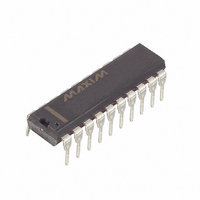
DS1844-100 Maxim Integrated Products, DS1844-100 Datasheet

DS1844-100
Specifications of DS1844-100
Available stocks
Related parts for DS1844-100
DS1844-100 Summary of contents
Page 1
... Standard resistance values - DS1844-010 DS1844-050 DS1844-100 100 kW § Mixed resistor value combinations (contact factory for availability) § Operating Temperature Range - Industrial: -40°C to +85°C DESCRIPTION The DS1844 Quad Digital Potentiometer is a four-channel, digitally controlled linear potentiometer. Each potentiometer is comprised of 63 equi-resistive sections and has three terminals accessible to the user. ...
Page 2
... The DS1844 is a volatile device and will always power-up with the wiper positions set to mid-tap (position 32-decimal). The end-terminal H will have wiper position value 0-decimal. Because the DS1844 is a 64-position device only 6 bits of data are necessary to write a wiper’s value. However, communication with the DS1844 will require using a full 8 bits, with the remaining 2 bits specifying the potentiometer selected ...
Page 3
... The bus must be controlled by a master device which generates the serial clock (SCL), controls the bus access, and generates the START and STOP conditions. The DS1844 operates as a slave on the two-wire bus. Connections to the bus are made via the open-drain I/O lines SDA and SCL. ...
Page 4
... Slave transmitter mode: The 1 However, in this mode the direction bit will indicate that the transfer direction is reversed. Serial data is transmitted on SDA by the DS1844 while the serial clock is input on SCL. START and STOP conditions are recognized as the beginning and end of a serial transfer. ...
Page 5
... SLAVE ADDRESS A command/control byte is the 1 The command/control byte consists of a 4-bit control code. For the DS1844, this is set as 0101 binary for read/write operations. The next 3 bits of the command/ control byte are the device select bits or slave address (A2, A1, A0). They are used by the master device to select which of eight devices accessed ...
Page 6
... DS1844, potentiometer wiper data is transmitted to the DS1844 by the master device the case of the 5-wire serial protocol, a data byte for the DS1844 will contain potentiometer select data and wiper position value. The six least significant bits of data specify the wiper position value while the two most significant bits specify the potentiometer to be loaded ...
Page 7
ABSOLUTE MAXIMUM RATINGS* Voltage on Any Pin Relative to Ground Operating Temperature Storage Temperature Soldering Temperature * This is a stress rating only and functional operation of the device at these or any other conditions above those indicated in the ...
Page 8
ANALOG RESISTOR CHARACTERISTICS (-40°C to +85°C; V PARAMETER SYMBOL End-to-End Resistor Tolerance Absolute Linearity Relative Linearity -3dB Cutoff frequency Temperature Coefficent 2-WIRE ADDRESSABLE INTERFACE AC ELECTRICAL CHARACTERISTICS PARAMETER SYMBOL Port Select Setup SCL Clock Frequency Bus Free Time Between STOP ...
Page 9
SERIAL INTERFACE AC ELECTRICAL CHARACTERISTICS PARAMETER Port Select Setup R/ W Setup Clock Frequency Width of CLK Pulse Data Setup Time Data Hold Time Progapation Delay Time High to Low Level Clock to Output RST High to Clock Input ...
Page 10
... Resistor inputs cannot go below GND by more than 0.5 volts or above V volts. 13. -3dB cutoff frequency characteristics for the DS1844 depend on potentiometer total resistance: DS1844-010; 1 MHz; DS1844-050; 200 kHz; DS1844-100; 100 kHz. 14. See Figure 3, 5-wire timing diagram. 15. For 5-wire control logic and V = +0.6V. ...
Page 11
... DS1844 BLOCK DIAGRAM Figure 1 WIPER REGISTER CONFIGURATION Figure ...
Page 12
... SERIAL TIMING DIAGRAM Figure 3 (A), (B) (A) WRITING DATA TO THE DS1844 ...
Page 13
DATA TRANSFER OVERVIEW Figure 4 START COMMAND/CONTROL BYTE Figure 5 2-WIRE READ PROTOCOL Figure 6 2-WIRE WRITE PROTOCOLS Figure ...
Page 14
TIMING DIAGRAM Figure 8 DIGITAL OUTPUT LOAD Figure ...


