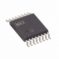
DS1859E-020+T&R Maxim Integrated Products, DS1859E-020+T&R Datasheet - Page 8

DS1859E-020+T&R
Manufacturer Part Number
DS1859E-020+T&R
Description
IC RES TEMP 20/20K 3MON 16-TSSOP
Manufacturer
Maxim Integrated Products
Datasheet
1.DS1859E-050.pdf
(28 pages)
Specifications of DS1859E-020+T&R
Taps
256
Resistance (ohms)
20K
Number Of Circuits
2
Temperature Coefficient
50 ppm/°C Typical
Memory Type
Non-Volatile
Interface
I²C, 2-Wire Serial
Voltage - Supply
2.85 V ~ 5.5 V
Operating Temperature
-40°C ~ 95°C
Mounting Type
Surface Mount
Package / Case
16-TSSOP
Resistance In Ohms
20K
Lead Free Status / RoHS Status
Lead free / RoHS Compliant
The user can read the registers that monitor the V
MON1, MON2, MON3, and temperature analog signals.
After each signal conversion, a corresponding bit is set
that can be monitored to verify that a conversion has
occurred. The signals also have alarm and warning flags
that notify the user when the signals go above or below
the user-defined value. Interrupts can also be set for
each signal.
The position values of each resistor can be indepen-
dently programmed. The user can assign a unique
value to each resistor for every 2°C increment over the
-40°C to +102°C range.
Dual, Temperature-Controlled Resistors with
Internally Calibrated Monitors
8
PIN
10
11
12
13
14
15
16
1
2
3
4
5
6
7
8
9
_____________________________________________________________________
BALL
B2
A2
C3
A1
B1
C2
C1
D1
D3
D4
C4
D2
B3
B4
A4
A3
NAME
MON1
MON2
MON3
WPEN
OUT1
OUT2
GND
SDA
SCL
V
IN1
IN2
H0
H1
L0
L1
CC
Detailed Description
2-Wire Serial Data I/O Pin. Transfers serial data to and from the device.
2-Wire Serial Clock Input. Clocks data into and out of the device.
Open-Drain Buffer Output
TTL/CMOS-Compatible Input to Buffer
Open-Drain Buffer Output
TTL/CMOS-Compatible Input to Buffer
Write Protect Enable. The device is not write protected if WPEN is connected to ground. This pin has
an internal pullup (R
Ground
External Analog Input
External Analog Input
External Analog Input
Low-End Resistor 0 Terminal. It is not required that the low-end terminals be connected to a potential
less than the high-end terminals of the corresponding resistor. Voltage applied to any of the resistor
terminals cannot exceed the power-supply voltage, V
High-End Resistor 0 Terminal. It is not required that the high-end terminals be connected to a
potential greater than the low-end terminals of the corresponding resistor. Voltage applied to any of
the resistor terminals cannot exceed the power-supply voltage, V
Low-End Resistor 1 Terminal
High-End Resistor 1 Terminal
Supply Voltage
WPEN
). See Table 6.
CC
,
Two buffers are provided to convert logic-level inputs
into open-drain outputs. Typically, these buffers are
used to implement transmit (Tx) fault and loss-of-signal
(LOS) functionality. Additionally, OUT1 can be asserted
in the event that one or more of the monitored values
go beyond user-defined limits.
FUNCTION
CC
, or go below ground.
CC
, or go below ground.
Pin Description


