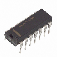
DS1807 Maxim Integrated Products, DS1807 Datasheet

DS1807
Specifications of DS1807
Available stocks
Related parts for DS1807
DS1807 Summary of contents
Page 1
... Each potentiometer has a total of 65 wiper positions including the mute position. Adjacent wiper positions are separated giving a total attenuation range of 64 dB. When the wipers are in the mute position, attenuation in excess achieved. The DS1807 also provides a zero-crossing detection capability. This capability eliminates noise caused by discrete wiper position changes ...
Page 2
... Because the DS1807 has 65 positions, only seven bits of data are needed to set a wiper’s position. Bits 0 through 5 of the register are used to set the position on the resistor array. Bit 6 is used to set the wiper position to the mute position and bit don’ ...
Page 3
... DS1807 BLOCK DIAGRAM Figure 1 WIPER REGISTER CONFIGURATION Figure DS1807 110499 ...
Page 4
... DS1807 has responded with an ACKNOWLEDGE after a “write potentiometer “ command. The STOP condition is discussed in the following section milliseconds the DS1807 has not detected a zero-crossing ( 0), the wiper position of the potentiometer(s) will change regardless of the state of the input signal. ...
Page 5
... Within the bus specifications a regular mode (100 kHz clock rate) and a fast mode (400 kHz clock rate) are defined. The DS1807 works in both modes. Acknowledge: Each receiving device, when addressed, is obliged to generate an acknowledge after the reception of each byte. The master device must generate an extra clock pulse which is associated with this acknowledge bit ...
Page 6
... A control byte is the first byte received following the START condition from the master device. The control byte consists of a 4-bit control code. For the DS1807, this is set as 0101 binary for read/write operations. The next 3 bits of the control byte are the device select bits (A2, A1, and A0). They are used by the master device to select which of eight devices are to be accessed ...
Page 7
... DS1807. Once the control byte has been issued and the master receives the acknowledgment from the DS1807, the command byte is transmitted to the DS1807. As mentioned above, there exist three write operations that can be used with the DS1807. The binary value of each write command is shown in Figure 7 and also in Table 1. ...
Page 8
... The control byte from the master device will follow the START condition. Once the control byte has been received by the DS1807, the part will respond with an ACKNOWLEDGE. The read/write bit of the control byte, as stated, should be set equal to 0 for writing the DS1807 ...
Page 9
... READ PROTOCOL Figure 6 2-READ READ PROTOCOL Figure DS1807 110499 ...
Page 10
... OL2 current C I/0 t Fast Mode (- +85 C) TYP MAX UNITS 5 +0 GND V GND+0.7 V =2.7V to 5.5V) CC TYP MAX UNITS 2000 µA +1 µA 400 1000 + 0.3V CC +10 µA µ 0 DS1807 NOTES 1 1 1,16 1,16 NOTES 3 1,2 1 110499 ...
Page 11
... BUF 4.7 t 0.6 HD:STA 4.0 t 1.3 LOW 4.7 t 0.6 HIGH 4 HD:DAT 0 t 100 SU:DAT 250 t 20+0. 20+0. 0.6 SU:STO 4 DS1807 =2.7V to 5.5V) CC MAX UNITS NOTES + +0.5 15 +0. kHz 14 ppm µV RMS =2.7V to 5.5V) CC MAX UNITS NOTES 400 kHz * 100 ** µ ...
Page 12
... These parameters are characterized and not 100% tested. 15. Interchannel matching is used to determine the relative difference in dB between the same position on each potentiometer. The DS1807 is specified for 0.5 dB Interchannel matching 16. See Figure 9. 17. Valid only. equal 3.0V and 5.0V and SDA and SCL are driven to the appropriate ...
Page 13
... TIMING DIAGRAM Figure 8 INTERNAL GROUND CONNECTIONS Figure 9 NOTE: GND and AGND must be tied to the same voltage level. DS1807 ORDERING INFORMATION ORDERING NUMBER DS1807 DS1807E 14L TSSOP (173-MIL) DS1807S 16L SOIC (300- MIL) PACKAGE OPERATING TEMPERATURE 14L DIP -40°C TO +85°C -40°C TO +85°C -40° ...


