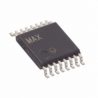
DS1859E-020+ Maxim Integrated Products, DS1859E-020+ Datasheet - Page 23

DS1859E-020+
Manufacturer Part Number
DS1859E-020+
Description
IC RES TEMP 20/20K 3MON 16-TSSOP
Manufacturer
Maxim Integrated Products
Datasheet
1.DS1859E-050.pdf
(28 pages)
Specifications of DS1859E-020+
Taps
256
Resistance (ohms)
20K
Number Of Circuits
2
Temperature Coefficient
50 ppm/°C Typical
Memory Type
Non-Volatile
Interface
I²C, 2-Wire Serial
Voltage - Supply
2.85 V ~ 5.5 V
Operating Temperature
-40°C ~ 95°C
Mounting Type
Surface Mount
Package / Case
16-TSSOP
Resistance In Ohms
20K
Lead Free Status / RoHS Status
Lead free / RoHS Compliant
An explanation of the binary search used to scale the
gain is best served with the following example pseudo-
code:
/* Assume that the Null input is 0.5V. */
/* In addition, the requirement for LSB is 50µV. */
/* Thus the null input 0.5V and the 90% of FS input is
2.949075V. */
See Right-Shifting section);
The gain register is now set and the resolution of the
conversion will best match the expected LSB. The next
step is to calibrate the offset of the DS1859. With the
correct gain value written to the gain register, again
force the null input to the pin. Read the digital result
from the part (Meas1). The offset value is equal to the
negative value of Meas1.
Offset
Dual, Temperature-Controlled Resistors with
FS = 65535 x 50E-6;
CNT1 = 0.5 / 50E-6;
CNT2 = 0.90 x FS / 50E-6;
Set the trim-offset-register to zero;
Set Right-Shift register to zero (typically zero.
gain_result = 0h;
Clamp = FFF8h/2^(Right_Shift_Register);
For n = 15 down to 0
begin
If Meas2 >= Clamp then
Else
end;
Set the gain register to gain_result;
_ Re
gister
gain_result = gain_result + 2^n;
Force the 90% FS input (2.949075V);
Meas2 = read the digital result from
the part;
gain_result = gain_result – 2^n;
Force the null input (0.5V);
Meas1 = read the digital result from
the part;
if (Meas2 – Meas1) > (CNT2 –
CNT1) then
gain_result = gain_result – 2^n;
4000
h
Meas
2
1
____________________________________________________________________
XOR
/* 3.27675 */
/* 10000 */
/* 58981.5 */
Internally Calibrated Monitors
4000
h
The calculated offset is now written to the DS1859 and
the gain and offset scaling is now complete.
The right-shifting method is used to regain some of the
lost ADC range of a calibrated system. If a system is
calibrated such that the maximum expected input
results in a digital output value of less than 7FFFh (1/2
FS), then it is a candidate for using the right-shifting
method.
If the maximum desired digital output is less than 7FFFh,
then the calibrated system is using less than 1/2 of the
ADC’s range. Similarly, if the maximum desired digital
output is less than 1FFFh, then the calibrated system is
only using 1/8 of the ADC’s range. For example, if using
a zero for the right-shift during internal calibration and
the maximum expected input results in a maximum digi-
tal output less than 1FFCh, only 1/8 of the ADC’s range is
used. If left like this, the three MS bits of the ADC will
never be used. In this example, a value of 3 for the right-
shifting will maximize the ADC range. No resolution is
lost since this is a 12-bit converter that is left justified.
The value can be right-shifted four times without losing
resolution. Table 9 shows when the right-shifting method
can be used.
Memory access from either device address can be
either read/write or read only. Write protection
is accomplished by a combination of control bits in
EEPROM (APEN and MPEN in configuration register
89h) and a write-protect enable (WPEN) pin. Since the
WPEN pin is often not accessible from outside the mod-
ule, this scheme effectively allows the module to be
locked by the manufacturer to prevent accidental writes
by the end user.
Separate write protection is provided for the Auxiliary
and Main Device address through distinct bits APEN
and MPEN. APEN and MPEN are bits from configura-
tion register 89h, Table 01. Due to the location, the
APEN and MPEN bits can only be written through the
Table 9. Right Shifting
WITH ZERO RIGHT-SHIFTS
OUTPUT RANGE USED
0h .. FFFFh
0h .. 7FFFh
0h .. 3FFFh
0h .. 1FFFh
0h .. 0FFFh
Right-Shifting A/D Conversion Result
(Scalable Dynamic Ranging)
RIGHT-SHIFTS NEEDED
Memory Protection
NUMBER OF
0
1
2
3
4
23


