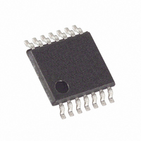
DS1845E-100+ Maxim Integrated Products, DS1845E-100+ Datasheet - Page 3

DS1845E-100+
Manufacturer Part Number
DS1845E-100+
Description
IC POT/MEM DUAL NV 100K 14-TSSOP
Manufacturer
Maxim Integrated Products
Datasheet
1.DS1845E-010.pdf
(14 pages)
Specifications of DS1845E-100+
Taps
100, 256
Resistance (ohms)
10K, 100K
Number Of Circuits
2
Temperature Coefficient
750 ppm/°C Typical
Memory Type
Non-Volatile
Interface
I²C, 2-Wire Serial
Voltage - Supply
2.7 V ~ 5.5 V
Operating Temperature
-40°C ~ 85°C
Mounting Type
Surface Mount
Package / Case
14-TSSOP
Resistance In Ohms
10K and 100K
Number Of Pots
Dual
Taps Per Pot
100
Resistance
100 KOhms
Wiper Memory
Non Volatile
Digital Interface
Serial (2-Wire)
Operating Supply Voltage
2.7 V to 5.5 V
Supply Current
40 uA
Maximum Operating Temperature
+ 85 C
Minimum Operating Temperature
- 40 C
Mounting Style
SMD/SMT
Supply Voltage (max)
5.5 V
Supply Voltage (min)
2.7 V
Tolerance
20 %
Lead Free Status / RoHS Status
Lead free / RoHS Compliant
DS1845 BLOCK DIAGRAM Figure 1
MEMORY ORGANIZATION
The DS1845’s serial EEPROM is internally organized with 256 words of 1 byte each. Each word requires
an 8-bit address for random word addressing. The byte at address F9h determines the wiper setting for
potentiometer 0, which contains 100 positions. Writing values above 63h to this address sets the wiper to
its uppermost position. The byte at address F8h determines the wiper setting for potentiometer 1, which
contains 256 positions (00h to FFh). The factory default wiper position for both potentiometers is FFh.
Memory locations 00h to F7h are factory programmed to 00h. Address locations FAh though FFh are
reserved and should not be written.
DEVICE OPERATION
Clock and Data Transitions: The SDA pin is normally pulled high with an external resistor or device.
Data on the SDA pin may only change during SCL low time periods. Data changes during SCL high
periods will indicate a start or stop conditions depending on the conditions discussed below. Refer to the
timing diagram Fig 2 for further details.
Start Condition: A high-to-low transition of SDA with SCL high is a start condition which must
precede any other command. Refer to the timing diagram Fig 2 for further details.
Stop Condition: A low-to-high transition of SDA with SCL high is a stop condition. After a read
sequence, the stop command places the DS1845 into a low-power mode. Refer to the timing diagram Fig
2 for further details.
Acknowledge: All address and data byte are transmitted via a serial protocol. The DS1845 pulls the
SDA line low during the ninth clock pulse to acknowledge that it has received each word.
Standby Mode: The DS1845 features a low-power mode that is automatically enabled after power-on,
after a stop command, and after the completion of all internal operations.
VCC
GND
SDA
SCL
WP
A0
A1
A2
2-WIRE
INTERFACE
CONTROL
DATA
248 BYTES
EEPROM
MEMORY
6 RESERVED
BYTES
1 BYTE WIPER
SETTING
POT 0
1 BYTE WIPER
SETTING
POT 1
3 of 14
POTENTIOMETER 0
POTENTIOMETER 1
Position
Position
100
256
Pot
Pot
H0
W0
L0
H1
W1
L1


