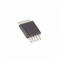
MAX5421BEUB+ Maxim Integrated Products, MAX5421BEUB+ Datasheet - Page 7

MAX5421BEUB+
Manufacturer Part Number
MAX5421BEUB+
Description
IC VOLTAGE DIVIDER DGLT 10MSOP
Manufacturer
Maxim Integrated Products
Datasheet
1.MAX5420AEUA.pdf
(9 pages)
Specifications of MAX5421BEUB+
Taps
4
Resistance (ohms)
15K
Number Of Circuits
1
Memory Type
Volatile
Interface
2-Wire Parallel
Voltage - Supply
4.75 V ~ 5.25 V, ±0.0 V ~ 5.25 V
Operating Temperature
-40°C ~ 85°C
Mounting Type
Surface Mount
Package / Case
10-MSOP, Micro10™, 10-uMAX, 10-uSOP
Resistance In Ohms
15K
Lead Free Status / RoHS Status
Lead free / RoHS Compliant
Temperature Coefficient
-
Figure 1. Simplified Functional Diagram
Figure 2. Switching Time Test Circuit
GND
R3B
R3A
0.1 F
RATIO = 8
0.1 F
+5V
-5V
R3B
V
V
R3A
DD
SS
RATIO = 8
H
L
R2B
R2A
_______________________________________________________________________________________
RATIO = 4
GENERATOR
PULSE
H
L
R2B
R2A
RATIO = 4
R1A
R1B
RATIO =
MAX5421
RATIO = 2
RATIO = 1
D1
(
1+
R_B
R_A
R1A
R1B
RATIO =
D0
Digitally Programmable Precision
)
RATIO = 2
RATIO = 1
W
(
1+
R_B
R_A
OSCILLOSCOPE FET
)
TEKTRONIX P6245
C
PROBE
L
1M
< 1pF
W
Voltage Divider for PGAs
Figure 4. Programmable-Gain Amplifier
The switching time of the MAX5420/MAX5421 depends
on the capacitive loading at W. For best performance,
reduce parasitic board capacitance by minimizing the
circuit board trace from W to the op amp inverting input,
and choose an op amp with low input capacitance.
TRANSISTOR COUNT: 118
PROCESS: CMOS
Figure 3. Programmable-Gain Amplifier with Op Amp Bias-
Current Matching
V
IN
MATCH_H
Switching Time and Layout Concerns
V
SS
GND
+5V
L
V
DD
L
V
+5V
SS
MAX5421
V
W
DD
GND
W
V
MAX5420
IN
H
MATCH_L
Chip Information
MAX4237
H
+5V
MAX4493
+5V
V
OUT
V
OUT
7


