AD5245BRJ10-R2 Analog Devices Inc, AD5245BRJ10-R2 Datasheet - Page 2
AD5245BRJ10-R2
Manufacturer Part Number
AD5245BRJ10-R2
Description
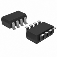
IC POT DGTL 10K 256POS SOT23-8
Manufacturer
Analog Devices Inc
Datasheet
1.AD5245BRJZ100-RL7.pdf
(20 pages)
Specifications of AD5245BRJ10-R2
Rohs Status
RoHS non-compliant
Taps
256
Resistance (ohms)
10K
Number Of Circuits
1
Temperature Coefficient
45 ppm/°C Typical
Memory Type
Volatile
Interface
I²C, 2-Wire Serial
Voltage - Supply
2.7 V ~ 5.5 V
Operating Temperature
-40°C ~ 125°C
Mounting Type
Surface Mount
Package / Case
SOT-23-8
Resistance In Ohms
10K
Number Of Elements
1
# Of Taps
256
Resistance (max)
10KOhm
Power Supply Requirement
Single
Interface Type
Serial (2-Wire/I2C)
Single Supply Voltage (typ)
3/5V
Dual Supply Voltage (typ)
Not RequiredV
Single Supply Voltage (min)
2.7V
Single Supply Voltage (max)
5.5V
Dual Supply Voltage (min)
Not RequiredV
Dual Supply Voltage (max)
Not RequiredV
Operating Temp Range
-40C to 125C
Operating Temperature Classification
Automotive
Mounting
Surface Mount
Pin Count
8
For Use With
AD5245EVAL - BOARD EVAL FOR AD5245
Lead Free Status / RoHS Status
Not Compliant
Other names
AD5245BRJ10-R2TR
Available stocks
Company
Part Number
Manufacturer
Quantity
Price
Company:

Part Number:
AD5245BRJ10-R2
Manufacturer:
AD
Quantity:
11 560


AD5245
TABLE OF CONTENTS
Features .............................................................................................. 1
Applications....................................................................................... 1
Functional Block Diagram .............................................................. 1
Pin Configuration............................................................................. 1
General Description ......................................................................... 1
Revision History ............................................................................... 2
Electrical Characteristics ................................................................. 3
Timing Characteristics..................................................................... 5
Absolute Maximum Ratings............................................................ 6
Pin Configuration and Function Descriptions............................. 7
Typical Performance Characteristics ............................................. 8
REVISION HISTORY
1/06—Rev. A to Rev. B
Changes to Table 3........................................................................... 5
Changes to Ordering Guide ......................................................... 19
3/04—Rev. 0 to Rev. A
Updated Format................................................................ Universal
Changes to Features......................................................................... 1
Changes to Applications ................................................................. 1
Changes to Figure 1......................................................................... 1
Changes to Electrical Characteristics—5 kΩ Version ................ 3
Changes to Electrical Characteristics—10 kΩ, 50 kΩ,
and 100 kΩ Versions ....................................................................... 4
Changes to Timing Characteristics ............................................... 5
Changes to Absolute Maximum Ratings ...................................... 6
Moved ESD Caution to Page .......................................................... 6
Changes to Pin Configuration and Function Descriptions ....... 7
Changes to Figures 22 and 23 ...................................................... 11
Moved Figure 25 to Figure 26 ...................................................... 11
Moved Figure 26 to Figure 27 ...................................................... 11
Moved Figure 27 to Figure 25 ...................................................... 11
Deleted Figures 31 and 32 ............................................................ 12
Changes to Figure 32, Figure 33 and Figure 34 ......................... 12
Changes to Rheostat Operation Section..................................... 13
Added Figure 35............................................................................. 13
Changes to Equation 1 and Equation 2 ...................................... 13
Changes to Table 6 and Table 7.................................................... 13
5 kΩ Version.................................................................................. 3
10 kΩ, 50 kΩ, 100 kΩ Versions .................................................. 4
5 kΩ, 10 kΩ, 50 kΩ, 100 kΩ Versions........................................ 5
ESD Caution.................................................................................. 6
Rev. B | Page 2 of 20
Test Circuits..................................................................................... 12
Theory of Operation ...................................................................... 13
I C Interface
Outline Dimensions ....................................................................... 19
Added Figure 37 ............................................................................ 14
Changes to Equation 4 .................................................................. 14
Deleted Readback RDAC Value Section .................................... 14
Deleted Level Shifting for Bidirectional Interface Section ...... 14
Moved ESD Protection Section to Page ..................................... 14
Changes to Figure 38 and Figure 39............................................ 14
Moved Terminal Voltage Operating Range Section to Page.... 14
Changes to Figure 40..................................................................... 14
Moved Power-Up Sequence Section to Page ............................. 14
Moved Layout and Power Supply Bypassing Section to Page . 15
Added Constant Bias to Retain Resistance Setting Section..... 15
Added Figure 42 ............................................................................ 15
Added Evaluation Board Section ................................................ 15
Added Figure 43 ............................................................................ 15
Moved I
Changes to I2C Compatible 2-Wire Serial Bus Section ........... 16
Moved Table 5 and Table 6 to Page ............................................. 17
(Renumbered as Table 8 and Table 9)
Moved Figure 36, Figure 37, and Figure 38 to Page.................. 17
(Renumbered as Figure 44, Figure 45, and Figure 46)
Moved Multiply Devices on One Bus Section to Page ............. 18
Updated Ordering Guide ............................................................. 19
Updated Outline Dimensions...................................................... 19
Moved I
5/03—Revision 0: Initial Version
2
Programming the Variable Resistor......................................... 13
Programming the Potentiometer Divider............................... 14
ESD Protection ........................................................................... 14
Terminal Voltage Operating Range ......................................... 14
Power-Up Sequence ................................................................... 14
Layout and Power Supply Bypassing ....................................... 14
Constant Bias to Retain Resistance Setting............................. 15
Evaluation Board ........................................................................ 15
I C-Compatible 2-Wire Serial Bus
Ordering Guide .......................................................................... 19
2
2
2
C Interface Section to Page........................................... 16
C Disclaimer to Page ..................................................... 20
.................................................................................... 16
........................................... 16
Related parts for AD5245BRJ10-R2
Image
Part Number
Description
Manufacturer
Datasheet
Request
R

Part Number:
Description:
256-Position I2C Compatible Digital Potentiometer
Manufacturer:
Analog Devices
Datasheet:

Part Number:
Description:
±1.7g Dual-Axis IMEMS Accelerometer Evaluation Board
Manufacturer:
Analog Devices Inc
Datasheet:

Part Number:
Description:
Inertial Sensor Evaluation System
Manufacturer:
Analog Devices Inc
Datasheet:
Part Number:
Description:
Manufacturer:
Analog Devices Inc
Datasheet:
Part Number:
Description:
Manufacturer:
Analog Devices Inc
Datasheet:
Part Number:
Description:
Manufacturer:
Analog Devices Inc
Datasheet:
Part Number:
Description:
Manufacturer:
Analog Devices Inc
Datasheet:
Part Number:
Description:
Manufacturer:
Analog Devices Inc
Datasheet:
Part Number:
Description:
Manufacturer:
Analog Devices Inc
Datasheet:
Part Number:
Description:
Manufacturer:
Analog Devices Inc
Datasheet:
Part Number:
Description:
Manufacturer:
Analog Devices Inc
Datasheet:
Part Number:
Description:
Manufacturer:
Analog Devices Inc
Datasheet:
Part Number:
Description:
Manufacturer:
Analog Devices Inc
Datasheet: