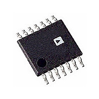
AD5260BRU20-REEL7 Analog Devices Inc, AD5260BRU20-REEL7 Datasheet - Page 13

AD5260BRU20-REEL7
Manufacturer Part Number
AD5260BRU20-REEL7
Description
IC DGTL POT SNGL 256POS 14-TSSOP
Manufacturer
Analog Devices Inc
Specifications of AD5260BRU20-REEL7
Rohs Status
RoHS non-compliant
Taps
256
Resistance (ohms)
20K
Number Of Circuits
1
Temperature Coefficient
35 ppm/°C Typical
Memory Type
Volatile
Interface
4-Wire SPI Serial
Voltage - Supply
4.5 V ~ 16.5 V, ±4.5 V ~ 5.5 V
Operating Temperature
-40°C ~ 85°C
Mounting Type
Surface Mount
Package / Case
14-TSSOP
Resistance In Ohms
20K
Number Of Elements
1
# Of Taps
256
Resistance (max)
20KOhm
Power Supply Requirement
Single/Dual
Interface Type
Serial (4-Wire/SPI)
Single Supply Voltage (typ)
15V
Dual Supply Voltage (typ)
±5V
Single Supply Voltage (min)
4.5V
Single Supply Voltage (max)
16.5V
Dual Supply Voltage (min)
±4.5V
Dual Supply Voltage (max)
±5.5V
Operating Temp Range
-40C to 85C
Operating Temperature Classification
Industrial
Mounting
Surface Mount
Pin Count
14
Lead Free Status / RoHS Status
Not Compliant
TEST CIRCUITS
Test Circuits 1 to 9 define the test conditions used in the product specification table.
REV. 0
0.01
100
0.1
10
1
0
Test Circuit 2. Resistor Position Nonlinearity Error
(Rheostat Operation; R-INL, R-DNL)
V
T
A
A
TPC 27. I
V
32
= V
= 25 C
MS2
B
Test Circuit 1. Potentiometer Divider
Nonlinearity Error (INL, DNL)
= OPEN
64
Test Circuit 3. Wiper Resistance
R
AB
CODE – Decimal
V
96
= 50k
MAX
A
B
NC
DUT
128 160 192 224
R
A
DUT
B
AB
vs. Code
W
A
B
DUT
W
= 20k
W
NC = NO CONNECT
R
AB
V
W
= 200k
V
MS1
V+ = V
1LSB = V+/2
I
W
V
= V
256
MS
DD
R
V
DD
MS
W
I
= [V
W
/R
N
NOMINAL
MS1
TPC 28. Long-Term Resistance Drift
– V
–0.05
–0.10
–0.15
–0.20
MS2
0.10
0.05
0
]/I
0
W
CODE = 80
V
SS = 135 UNITS
DD
50
HOURS OF OPERATION AT 150 C
= V
100
SS
150
=
H
5V
200 250 300 350 400 450
–13–
Test Circuit 4. Power Supply Sensitivity (PSS, PSSR)
Test Circuit 7. Common-Mode Leakage Current
AVG –3
AVG +3
V+
OFFSET
Test Circuit 6. Incremental ON Resistance
AVG
GND
Test Circuit 5. Gain vs. Frequency
500
V
V
DUT
V
DD
V
DD
SS
IN
V
A
A
A = NC
B
GND
DUT
B
W
W
DUT
NC
NC
A
B
40
30
20
10
I
TPC 29. Channel-to-Channel
Resistance Matching (AD5262)
B
SW
A
0
W
–0.50
V
SS
CHANNEL-TO-CHANNEL R
R
CODE = 00
CODE SET TO MID-SCALE
T
3 LOTS
SAMPLE SIZE = 135
A
SW
W
TO V
V
= 150 C
–0.40 –0.30 –0.20 –0.10
MS
PSRR (dB) = 20 LOG
PSS (%/%) =
=
V+ = V
AD5260/AD5262
0.1V
DD
I
SW
I
CM
AD8610
DD
H
–13V
+13V
0.1V
10%
V
V
MS
DD
V
%
%
CM
(
V
AB
OUT
0
V
V
MATCH – %
MS
DD
0.10 0.20
)


