AD7376AN100 Analog Devices Inc, AD7376AN100 Datasheet
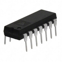
IC DIGITAL POT 14-DIP

AD7376AN100

Manufacturer Part Number
AD7376AN100
Description
IC DIGITAL POT 14-DIP
Manufacturer
Analog Devices Inc
Datasheets

Specifications of AD7376AN100

Rohs Status
RoHS non-compliant
Taps
128
Resistance (ohms)
100K
Number Of Circuits
1
Temperature Coefficient
300 ppm/°C Typical
Memory Type
Volatile
Interface
SPI, 3-Wire Serial
Voltage - Supply
4.5 V ~ 33 V, ±4.5 V ~ 16.5 V
Operating Temperature
-40°C ~ 85°C
Mounting Type
Through Hole
Package / Case
14-DIP (0.300", 7.62mm)
Resistance In Ohms
100K
Number Of Elements
1
# Of Taps
128
Resistance (max)
100KOhm
Power Supply Requirement
Single/Dual
Interface Type
Serial (3-Wire/SPI)
Single Supply Voltage (typ)
5/9/12/15/18/24V
Dual Supply Voltage (typ)
±5/±15V
Single Supply Voltage (min)
4.5V
Single Supply Voltage (max)
28V
Dual Supply Voltage (min)
±4.5V
Dual Supply Voltage (max)
±16.5V
Operating Temp Range
-40C to 85C
Operating Temperature Classification
Industrial
Mounting
Through Hole
Pin Count
14
Lead Free Status / RoHS Status
Not Compliant
a
GENERAL DESCRIPTION
The AD7376 provides a single channel, 128-position digitally-
controlled variable resistor (VR) device. This device performs the
same electronic adjustment function as a potentiometer or vari-
able resistor. These products were optimized for instrument and
test equipment applications where a combination of high voltage
with a choice between bandwidth or power dissipation are avail-
able as a result of the wide selection of end-to-end terminal resis-
tance values. The AD7376 contains a fixed resistor with a wiper
contact that taps the fixed resistor value at a point determined by
a digital code loaded into the SPI-compatible serial-input regis-
ter. The resistance between the wiper and either endpoint of the
fixed resistor varies linearly with respect to the digital code trans-
ferred into the VR latch. The variable resistor offers a completely
programmable value of resistance between the A terminal and the
wiper or the B terminal and the wiper. The fixed A to B terminal
resistance of 10 k , 50 k , 100 k or 1 M has a nominal tem-
perature coefficient of –300 ppm/ C.
The VR has its own VR latch which holds its programmed resis-
tance value. The VR latch is updated from an internal serial-to-
parallel shift register which is loaded from a standard 3-wire
serial-input digital interface. Seven data bits make up the data
word clocked into the serial data input register (SDI). Only the
last seven bits of the data word loaded are transferred into the
7-bit VR latch when the CS strobe is returned to logic high. A
serial data output pin (SDO) at the opposite end of the serial
register allows simple daisy-chaining in multiple VR applications
without additional external decoding logic.
The reset (RS) pin forces the wiper to the midscale position by
loading 40
*Patent Number: 5495245
REV. 0
Information furnished by Analog Devices is believed to be accurate and
reliable. However, no responsibility is assumed by Analog Devices for its
use, nor for any infringements of patents or other rights of third parties
which may result from its use. No license is granted by implication or
otherwise under any patent or patent rights of Analog Devices.
FEATURES
128 Position
Potentiometer Replacement
10 k , 50 k , 100 k , 1 M
Power Shutdown: Less than 1 A
3-Wire SPI Compatible Serial Data Input
+5 V to +30 V Single Supply Operation
Midscale Preset
APPLICATIONS
Mechanical Potentiometer Replacement
Instrumentation: Gain, Offset Adjustment
Programmable Voltage-to-Current Conversion
Programmable Filters, Delays, Time Constants
Line Impedance Matching
Power Supply Adjustment
5 V to
H
into the VR latch. The SHDN pin forces the resistor
15 V Dual Supply Operation
to an end-to-end open circuit condition on the A terminal and
shorts the wiper to the B terminal, achieving a microwatt power
shutdown state. When shutdown is returned to logic high, the
previous latch settings put the wiper in the same resistance
setting prior to shutdown as long as power to V
moved. The digital interface is still active in shutdown so that
code changes can be made that will produce a new wiper posi-
tion when the device is taken out of shutdown.
The AD7376 is available in both surface mount (SOL-16) and
the 14-lead plastic DIP package. For ultracompact solutions
selected models are available in the thin TSSOP package. All
parts are guaranteed to operate over the extended industrial
temperature range of –40 C to +85 C. For operation at lower
supply voltages (+3 V to +5 V), see the AD8400/AD8402/
AD8403 products.
The last seven data bits clocked into the serial input register will
be transferred to the VR 7-bit latch when CS returns to logic
high. Extra data bits are ignored.
One Technology Way, P.O. Box 9106, Norwood, MA 02062-9106, U.S.A.
Tel: 781/329-4700
Fax: 781/326-8703
(DATA OUT)
(DATA IN)
V
OUT
SDO
CLK
SDI
CS
CLK
SDO
SDI
t
V
CS
CSH0
DD
0V
1
0
1
0
1
0
1
0
FUNCTIONAL BLOCK DIAGRAM
Figure 1. Detail Timing Diagram
AD7376
t
CSS
D
Q
GND
REGISTER
World Wide Web Site: http://www.analog.com
Digital Potentiometer
D
SERIAL
7-BIT
X
D'
t
CH
X
CK
t
DS
7
t
CL
D'
LATCH
X
7-BIT
15 V Operation
D
t
DH
RS
R
X
t
1 LSB ERROR BAND
© Analog Devices, Inc., 1997
CSH
7
AD7376*
SHDN
SHDN
t
t
DD
PD_MAX
CS1
t
is not re-
S
t
CSW
V
W
V
A
B
DD
SS
1 LSB

Related parts for AD7376AN100

AD7376AN100 Summary of contents

Page 1

FEATURES 128 Position Potentiometer Replacement 100 Power Shutdown: Less than 1 A 3-Wire SPI Compatible Serial Data Input + +30 V Single Supply Operation ...

Page 2

AD7376–SPECIFICATIONS ELECTRICAL CHARACTERISTICS Parameter DC CHARACTERISTICS RHEOSTAT MODE (Specifications Apply to All VRs) 2 Resistor Differential NL 2 Resistor Nonlinearity Nominal Resistor Tolerance Resistance Temperature Coefficient Wiper Resistance Wiper Resistance DC CHARACTERISTICS POTENTIOMETER DIVIDER MODE (Specifications Apply to All VRs) ...

Page 3

... SOIC (SOL-16 120 C/W TSSOP- 240 C/W Model AD7376AN10 AD7376AR10 AD7376ARU10 AD7376AN50 AD7376AR50 AD7376ARU50 AD7376AN100 AD7376AR100 AD7376ARU100 AD7376AN1M AD7376AR1M AD7376ARU1M Die Size: 101.6 mil 127.6 mil, 2.58 mm 3.24 mm Number Transistors: 840 CAUTION ESD (electrostatic discharge) sensitive device. Electrostatic charges as high as 4000 V readily accumulate on the human body and test equipment and can discharge without detection ...

Page 4

Performance Characteristics AD7376 100 128 CODE – Decimal Figure 2. Wiper To End Terminal Percent Resistance vs. Code +15V –15V ...

Page 5

– 0.05 0 –0. +15V –15V –0. +2. +85 C –0. ...

Page 6

AD7376 CODE = 40H –6 20H –12 10H –18 08H –24 04H –30 02H –36 01H – +15V –15V SS – 50mVrms AMPL B OP275 R = 100k ...

Page 7

V = + 1.0 0 SUPPLY VOLTAGE (V Figure 29. Input Logic Threshold Voltage vs. V Supply Voltage DD 1600 1200 800 V ...

Page 8

AD7376 R SW CODE = OO DUT Figure 38. Incremental ON Resistance Test Circuit DUT V B GND SS NC Figure 39. Common-Mode Leakage Current ...

Page 9

Table II (DEC Output State 127 74 Full-Scale 64 5035 Midscale ( Condition) 1 9996 1 LSB 0 10035 Zero-Scale The typical distribution of R from device to device matching BA is process ...

Page 10

AD7376 The data setup and data hold times in the specification table determine the data valid time requirements. The last seven bits of the data word entered into the serial register are held when CS returns high. At the same ...

Page 11

Plastic DIP (N-14) 0.795 (20.19) 0.725 (18.42 0.280 (7.11) 0.240 (6.10 0.060 (1.52) PIN 1 0.015 (0.38) 0.210 (5.33) MAX 0.130 (3.30) 0.160 (4.06) MIN 0.115 (2.93) SEATING 0.022 (0.558) 0.100 0.070 (1.77) PLANE (2.54) ...

Page 12

–12– ...

Related keywords